Daniel is joined by John O’Donnell, Founder and CEO of yieldHUB, a pioneering leader in advanced data analytics for the semiconductor industry. Since establishing the company in 2005 he has transformed it from a two-person startup into a trusted multinational partner that empowers some of the world’s leading semiconductor … Read More
Dan is joined by Kevin Robinson, yieldHUB’s Vice President of operations and sales. With over 23 years of experience as a test engineer in the semiconductor industry, Kevin brings a wealth of knowledge and dedication to his dual role. At yieldHUB, Kevin leads both sales and operations teams, playing a crucial role in delivering… Read More
Dan is joined by Carl Moore, a semiconductor and yield management expert with a career spanning 40 years. Carl’s held technical management positions across product and test engineering, assembly, manufacturing, and design at established semiconductor companies. Carl is passionate about data analytics and has a reputation… Read More
Collecting and analyzing semiconductor test data is a subject that holds a special place for me. Developing a factory data collection and analysis system was my first job out of school. The company was RCA, and the factories were in Findlay, Ohio (analog/mixed signal) and West Palm Beach, Florida (digital). There was a pilot… Read More
I recently had the pleasure of attending the AI Hardware Summit at the Computer History Museum in Mountain View, CA. This two-day conference brought together many companies involved in building artificial intelligence solutions. Though the focus was on building the hardware for this area, there was naturally much discussion… Read More
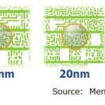
It is truly amazing to consider the advances in microelectronic process development, using 193i photolithography. The figure below is a stark reminder of the difference between the illuminating wavelength and the final imaged geometries. This technology evolution has been enabled by continued investment in mask data generation… Read More
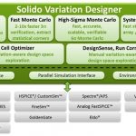
With the insatiable wafer appetites of the fabless semiconductor companies in the mobile space, yield has never been more critical. The result being better EDA tools every year and this blog highlights one of the many examples. It has been a pleasure writing about Solido Design Automation and seeing them succeed amongst the foundries… Read More
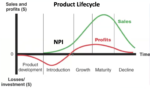
Since the beginning of the semiconductor industry, improving the rate of yield learning has been a critical factor in the success silicon manufacturing. Each fab has dedicated yield teams that look at the yield of wafers manufactured the previous day and attempt to find the root cause of any unexpected “excursions.” In earlier… Read More
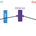
Yield, no topic is more important to the semiconductor ecosystem. After spending a significant part of my career on Design for Manufacturability (DFM) and Design for Yield (DFY), I’m seriously offended when semiconductor professionals make false and misleading statements that negatively affects the industry that … Read More