Collecting and analyzing semiconductor test data is a subject that holds a special place for me. Developing a factory data collection and analysis system was my first job out of school. The company was RCA, and the factories were in Findlay, Ohio (analog/mixed signal) and West Palm Beach, Florida (digital). There was a pilot manufacturing line in Somerville, New Jersey as well. The chips built by these fabs were used, among other things, to build RCA television sets in Bloomington, Indiana.
The world has changed a lot in a seemingly short period of time. The work going on back then at RCA is no longer done in this country for the most part. The data analysis system I worked on was based on IBM mainframe technology, dedicated communication lines for data access and batch processing for results. A lot has changed here as well. Recently, Dan Nenni published an interview with John O’Donnel, the CEO of yieldHUB. The company offers a contemporary, cloud-based technology to gather real-time data from semiconductor manufacturing and test, validate and clean the data and then provide actionable insights into the devices being tracked. I only dreamed about this kind of capability at RCA.
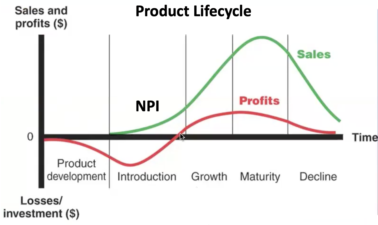
The yieldHUB platform offers several use models, including NPI, Production, Advanced Production and Custom. I’d like to focus in this post on NPI, or new product introduction. This is the process of bringing up a new design in the target system with the goal of validating its readiness to move to volume manufacturing, the stage where everyone starts making money.
There are many capabilities offered in the NPI use model from yieldHUB. Here is a list of them:
|
Bin analysis |
Bin galleries, stacking of wafer maps, trends |
|
Calculated Tests/Multivariate analysis |
Create tests from other tests, e.g., test1/test2 or test1 with different set of limits. Done virtually in the database |
|
Characterization |
Fully understand the variations in behavior of your new silicon due to changes in material or test conditions |
|
Gage R&R |
Make your program insensitive to setup with a highly visual gage R&R tool |
|
Indexed correlation/drift analysis |
Population drift analysis and per die drift analysis across wafer sort or packaged test strips |
|
Parametric analysis |
Analyze parameters and tests in detail, including and applying filters |
|
Sensitivity analysis |
Which tests are most sensitive to a change in test program? Might reveal something unexpected |
|
Test time analysis |
Do you store test time in your data logs? |
|
Virtual Re-rest |
Tweak test limits in simulation mode and investigate the effect on yield |
The Gage R&R item may not familiar to some readers. Here is a description of it from the yieldHUB website:
Gage R&R has been used for many years in the semiconductor industry to measure variation during test for repeatability and reproducibility. These measurements are then used to assess the suitability of the test for production. But often the focus is on qualifying tests on one site, only leaving issues for production when multi-site testing is used.
The write-up goes on to show an example of a parameter where the site 2 measurements are different from the other sites and give many false fails. This example would fail Gage R&R.
yieldHub also did a webinar to provide more detail on how to perform new product introduction. In 25 minutes, this webinar covered a lot of ground. It is presented by John O’Donnel, Founder and CEO and Kevin Robinson, Director of Customer Success. After a short overview of yieldHUB, the details of NPI are discussed. The primary goals of NPI are stated as:
- Fastest time to market
- Tightest specs
- Highest yield
This sums it up quite well. Characterization is a key part of NPI and the webinar’s definition of this step is worth repeating:
“The goal of characterization is to make sure that the variation in parametric behavior due to allowed changes in material or test conditions is understood early.”
Share this post via:


Comments
2 Replies to “How yieldHUB Helps Bring a New Product to Market”
You must register or log in to view/post comments.