![]()
We all know that building advanced semiconductors is a team sport. Many design parameters and processes must come together in a predictable, accurate and well-orchestrated way to achieve success. The players are diverse and cover the globe. Assembling all the information required to optimize the project in one place, with the right level of analysis and insight is a particularly vexing problem. My first job out of college was building such a system for internal use at the RCA Solid State Division (RIP). If you happen to have a copy of the 15thDesign Automation Conference Proceedings handy, thumb to page 117 to check out my early efforts. That was back in the dawn of time when infrastructure was thin, and automaton was non-existent. This early work gave me an appreciation for the tools that followed over the decades. Today, optimizing designs is still difficult, but there are some excellent systems that cut the problem down to size. Let’s examine how yieldHUB improves semiconductor product quality for all.
What’s The Problem?
Let me begin by framing the problem. It’s well known that many companies all over the world are involved in the design and manufacture of advanced chips. Design, verification, wafer fab, packaging, final test, qualification, and in-system validation and bring-up are all highly complex processes that involve many tools and companies around the world.
To ensure harmonious operation between all these entities requires, first and foremost, visibility into the data produced by each step. Here is the first problem – all sources of data have a particular format and access method. It would be nice if they were all the same, but they are not. So, there is a many-to-many challenge to assemble all the data needed in one place that is reliable and accurate. The single source of truth that is the holy grail for many online systems.
Once this is achieved, the next problem is what to do with all the data. What types of analyses are needed to turn data into useful information? The answer to that question depends on what you’re trying to monitor, debug or optimize. Many, many ways of looking at the data to find the needed insight must be supported. And we’re talking about massive amounts of information, making the whole process very challenging.
At the end of the day, product management teams need accessibility (all data in one place), analysis (a holistic view of everything important), coordination (everyone needs to be using the same information around the world), insight (the ability to spot the right trends), and support (to help use what’s available and quickly add something new when it’s needed).
Having been part of an internal team trying to solve this problem, I can tell you it’s too big for any internal team to address adequately. The cost of doing it right is too high for any one company.
An Elegant Solution
For almost twenty years, yieldHUB has been helping people working on yield improvement to enjoy their jobs and be more efficient. The company’s yield management platform and support organization have a worldwide footprint, both on-premise and in the cloud. Its data model is unique and hugely scalable, allowing customers to analyze data without having to download it first. The result is the ability to analyze hundreds of wafers worth of data in seconds. This is game-changing technology.

I recently had the opportunity to get a live tour of some of yieldHUB’s capabilities with Kevin Robinson, yieldHUB’s VP of operations. Based in the UK, Kevin has been building capabilities at yieldHUB to help customers conquer yield challenges for over ten years.
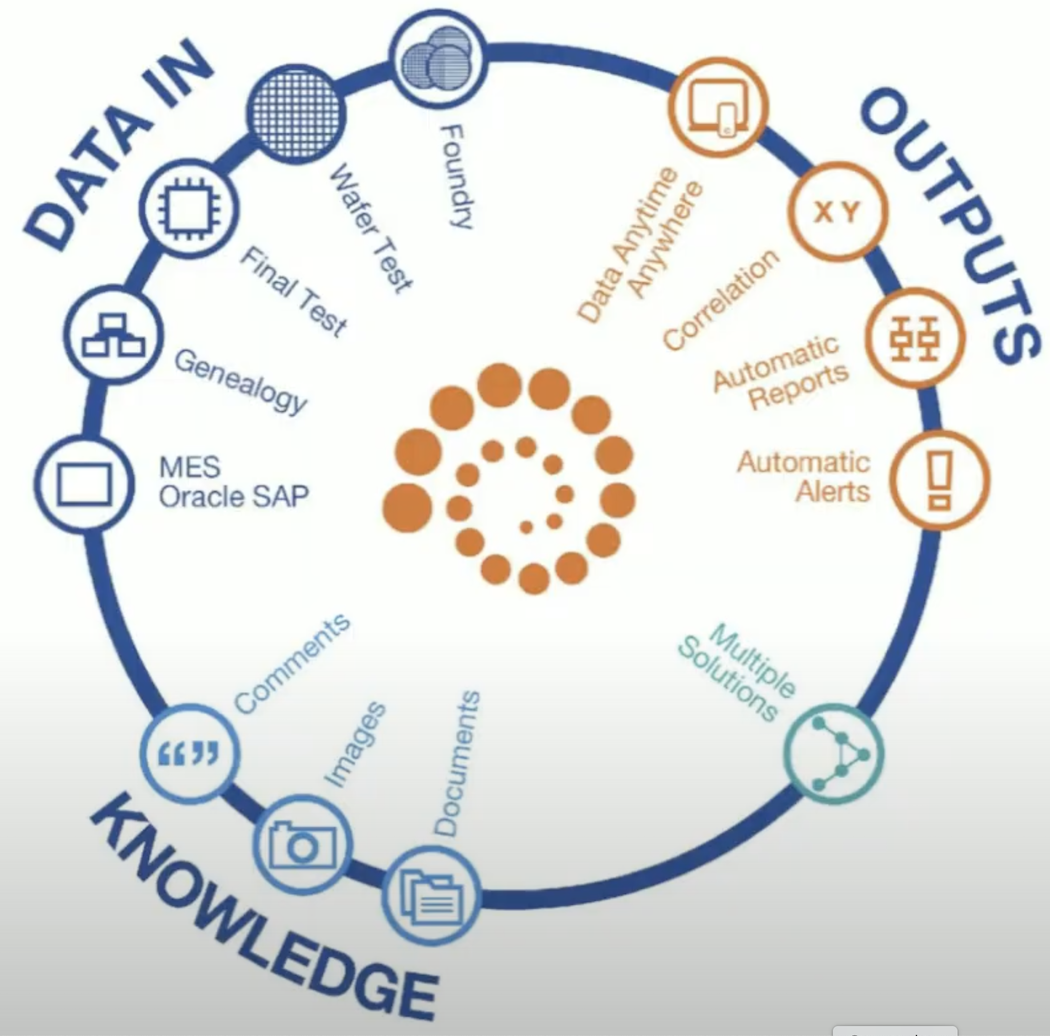
Kevin began by describing the breadth and depth of yieldHUB’s central data server system. Data is automatically consolidated from the foundry (WAT, wafer test, final test as well as in-line data from the fab line), PCB data, and module data for actual products shipping to end customers. This is supplemented with genealogy data and manufacturing execution/ERP data to create a complete view of the enterprise.
Using thin client technology, secure access to all this information for targeted analysis is possible either behind the firewall or in the cloud. A knowledge base allows information and comments to be attached to any part of the process and shared efficiently. For example, lot-level or product-level information in the knowledge base is automatically seen by all those working in that area of the enterprise. This saves a lot of time and dramatically improves collaboration.
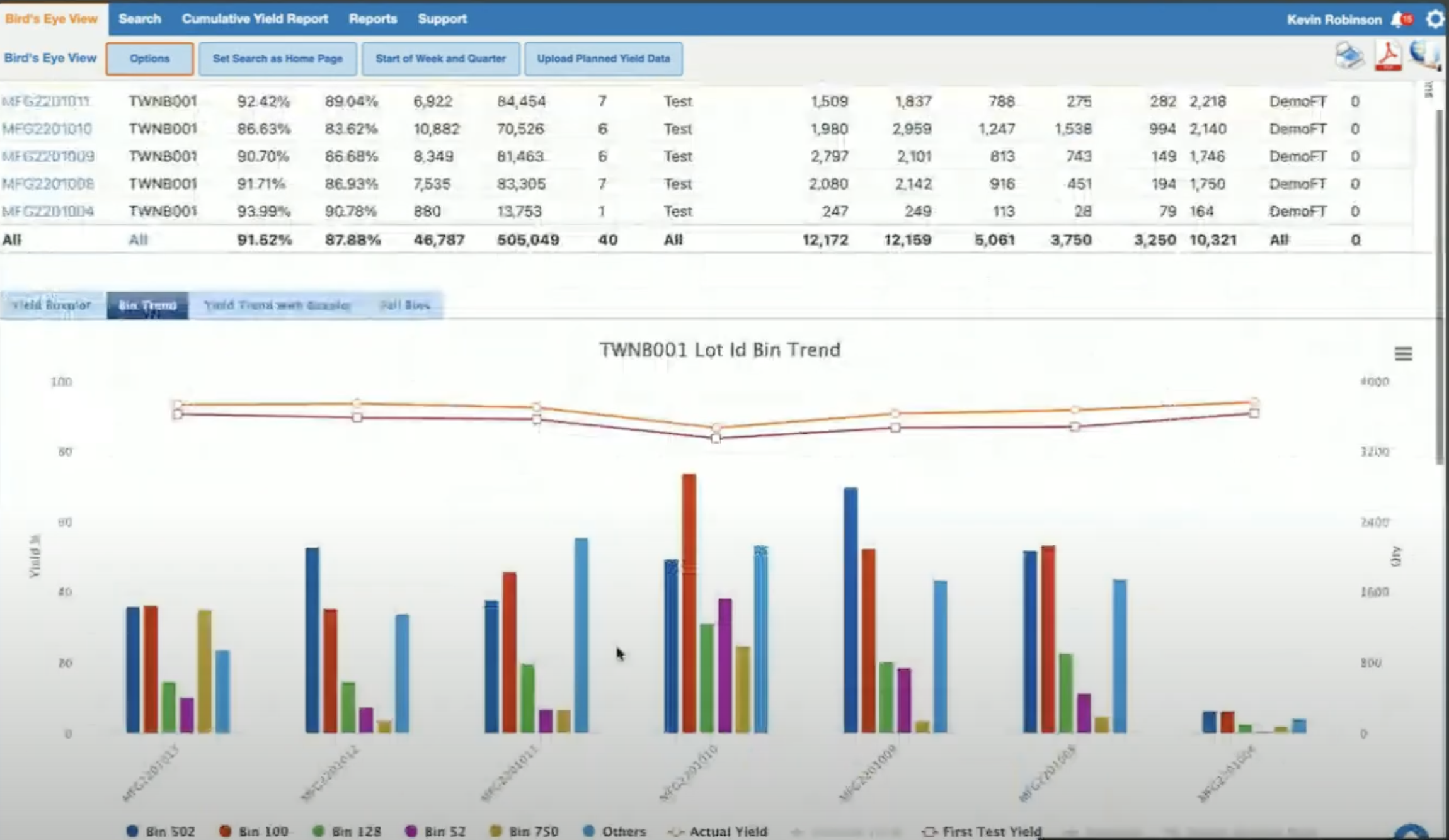
Kevin began by examining yield data for a half million mixed signal parts with embedded memory. This represents about 100GB of data. Each part is uniquely identified in the system, so there are many ways to explore the information. Kevin was able to quickly display this data to begin to identify possible trends. One example is shown below, where color-coded bar charts present failure mode distributions for various lots.

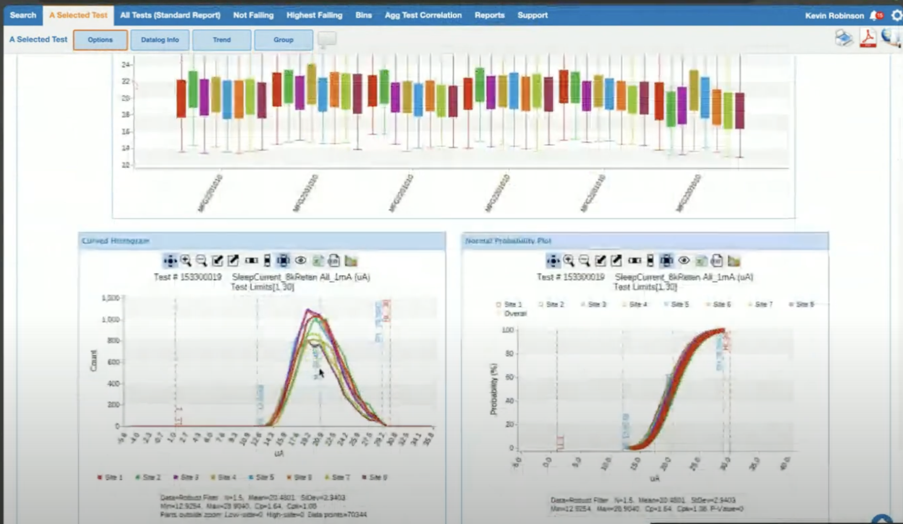
Kevin then began to drill down into this data with many views, generated in real-time. In the interest of time, I’ll show one example – analyzing the lowest yielding lot. Focusing on the highest failing test for that lot, he examined the behavior across test sites. That created a rich view of data relationships as shown in the figure below.


The data can also be displayed on a per-lot, per wafer basis to create wafer maps. An example is shown on the right. Kevin provided many more examples of how to explore and analyze this data and other large datasets.
From personal experience, I can testify that the easy-to-use analysis capabilities of this system hide a massive amount of implementation detail. Accurately acquiring data from so many different sources and making the resultant massive data sets accessible and easy to visualize and analyze is no small feat.
The diagram below summarizes the big picture view of yieldHUB and its impact on the enterprise.

To Learn More
If you care about yield and product quality, you need a system like this. If you’re considering building it yourself, let me emphatically suggest you take a different approach. It will take a lot longer than you think to implement, and the ever-changing supply chain dynamics, equipment profiles and analysis requirements will quickly consume way too much time and effort.
I’ve provided a small window into a very detailed demonstration. The good news is that you can set up your own tour of yieldHUB here. You can also view a recent webinar on collaboration and yield improvement here. And that’s the best way to learn how yieldHUB improves semiconductor product quality for all.
Share this post via:


Comments
There are no comments yet.
You must register or log in to view/post comments.