You are currently viewing SemiWiki as a guest which gives you limited access to the site. To view blog comments and experience other SemiWiki features you must be a registered member. Registration is fast, simple, and absolutely free so please,
join our community today!
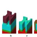
Establishing void-free fill of high aspect ratio TSVs, capped by a thin and uniform bulk layer optimized for removal by CMP, means fully optimizing each of a series of critical phases. As we will see in this 3-part series, the conditions governing outcomes for each phase vary greatly, and the complexity of interacting factors means… Read More
Establishing void-free fill of high aspect ratio TSVs, capped by a thin and uniform bulk layer optimized for removal by CMP, means fully optimizing each of a series of critical phases. As we will see in this 3-part series, the conditions governing outcomes for each phase vary greatly, and the complexity of interacting factors means… Read More
Extraction Features for 7nmby Tom Dillinger on 08-21-2017 at 12:00 pmCategories: Cadence, EDA, FinFET
Frequent Semiwiki readers are familiar with the importance of close collaboration between the foundries and EDA tool developers, to provide the crucial features required by new process nodes. Perhaps the best illustration of the significance of this collaboration is the technical evolution of layout parasitic extraction.… Read More
Founded in 1971 (2015: 45th year), SEMICON West 2015 is coming to the Moscone Center in San Francisco on from Tuesday, July 14[SUP]th[/SUP] to Thursday, July 16[SUP]th[/SUP]. SEMICON is the premier show for equipment and materials companies supporting the semiconductor, MEMS and solar industries.
The main ways to get value … Read More
It appears so. Why there is so much rush towards FD-SOI in recent days? Before talking about the game, let me reflect a bit on the FD-SOI technology first. The FD-SOI at 28nm claims to be the most power-efficient and lesser cost technology compared to any other technology available at that node. There are many other advantages from… Read More
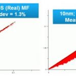
Results of TSMC’s ECO Fill Flowby Beth Martin on 12-22-2014 at 7:00 amCategories: EDA, TSMC
By Jeff Wilson, Mentor Graphics and Anderson Chiu, TSMC
At this year’s TSMC Open Innovation Platform® (OIP) Ecosystem Forum, Mentor Graphics and TSMC co-presented some results of the ECO Fill flow developed for TSMC customers working at advanced nodes. Here is a summary of the presentation. (TSMC customers can access the presentation… Read More
While FinFET yield controversy is going on, I see a lot being done to improve that yield by various means. One prime trend today, it must be, it’s worthwhile, is to pull up various signoffs as early as possible during the design cycle. And DFM signoff is a must with respect to yield of fabrication. This reminds me about my patents filed… Read More
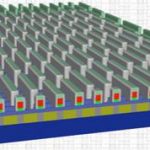
Metal fill requirements for inductors are now a fact of life. Fill has long been seen as detrimental to device performance due to parasitic capacitance. The necessity of fill arises from the need to ensure planarization of dielectric layers by using chemical mechanical polishing. Without adequate fill, areas of the chip can suffer… Read More
One of Coventor’s flagship products is SEMulator3D, and at Semicon West they announced a new version, 2014.100.
SEMulator3D is a powerful 3D semiconductor and MEMS process modeling platform. It uses highly efficient physics-driven voxel modeling technology. It models the physical effects of process steps, which is… Read More
Engineers are always looking to improve the efficiency of how they work, but don’t want to sacrifice accuracy in the process. This is true in the world of semiconductor process development, where traditional build-and-test cycles are both time and resource intensive. But what if there was a way to do certain steps in a ‘virtual’… Read More