You are currently viewing SemiWiki as a guest which gives you limited access to the site. To view blog comments and experience other SemiWiki features you must be a registered member. Registration is fast, simple, and absolutely free so please,
join our community today!
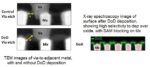
The further scaling of interconnect and via lithography for advanced nodes is challenged by the requirement to provide a process window that supports post-patterning critical dimension variations and mask overlay tolerances. At the recent international Electron Devices Meeting (IEDM) in San Francisco, TSMC presented … Read More
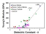
Of the three types of materials used in microelectronics – i.e., semiconductors, metals, and dielectrics – the first two often get the most attention. Yet, there is a pressing need for a rich variety of dielectric materials in device fabrication and interconnect isolation to satisfy the performance, power, and reliability … Read More
At SEMICON West, Applied Materials announced a new selective gap fill tool to address the growing resistance issues in interconnect at small dimensions. I had the opportunity to discuss this new tool and the applications for it with Zhebo Chen global product manager in the Metal Deposition Products group at Applied Materials.… Read More