TSMC recently held their 10th annual Open Innovation Platform (OIP) Ecosystem Forum. An earlier article summarized the highlights of the keynote presentation from L.C. Lu, TSMC Fellow and Vice-President, Design and Technology Platform, entitled “TSMC and Its Ecosystem for Innovation” (link).
One of the topics that L.C. discussed was the initiatives that TSMC pursued for the N3 process node, specifically for the High-Performance Computing (HPC) platform. This article provides more details about the design-technology co-optimization (DTCO) activities that resulted in performance gains for N3HPC, compared to the baseline N3 process. These details were provided by Y.K. Cheng, Director, Design Solution Exploration and Technology Benchmarking, in his presentation entitled “N3 HPC Design and Technology Co-Optimization”.
Background
Design technology co-optimization refers to a cooperative effort among process development engineering and circuit/IP design teams. The technology team optimizes the device and lithography process “window”, typically using TCAD process simulation tools. At advanced nodes, the allowed lithographic variability in line widths, spacings, uniformity, and density (and density gradient) is limited – technology optimization seeks to define the nominal fabrication parameters where the highly-dimensional statistical window maintains high yield. The circuit design team(s) evaluate the performance impacts of different lithographic topologies, extracting and annotating parasitic R and C elements to device-level netlist models.
A key element to DTCO is pursued by the library IP team. The standard cell “image” defines the allocated (vertical) dimension for nFET/pFET device widths and the number of (horizontal) wiring tracks available for intra-cell connections. The image also incorporates a local power distribution topology, with global power/ground grid connectivity requirements.
In addition to the library cell image, the increasing current density in the scaled metal wires at advanced nodes implies that DTCO includes process litho and circuit design strategies for contact/via connectivity. As the design variability in contact/via sizes is extremely limited due to litho/etch uniformity constraints, the process and circuit design teams focus on optimization of multiple, parallel contacts/vias and the associated metal coverage.
And, a critically important aspect of DTCO is the design and fabrication of the SRAM bitcell. Designers push for aggressive cell area lithography, combined with device sizing flexibility for sufficient read/write noise margins and performance (with a large number of dotted cells on the bitlines). Process engineers seek to ensure a suitable litho/etch window, and concurrently must focus on statistical tolerances during fabrication to support “high-sigma” robustness.
The fact that TSMC enables customers with foundation IP developed internally provides a tight DTCO development feedback loop.
N3HPC DTCO
Y.K. began his presentation highlighting the N3HPC DTCO results, using the power versus performance curves shown in the figure below. (The reference design block used for these comparisons is from an Arm A78 core; the curves span a range of supply voltages, at “typical” device characteristics.)
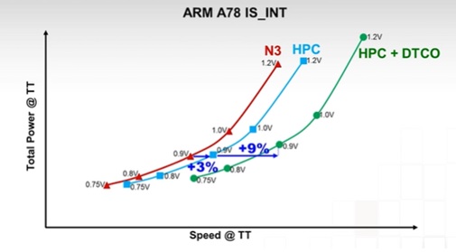
The collective set of optimizations provide an overall 12% performance boost over the baseline N3 offering. Note that (for the same supply voltage) the power dissipation increases slightly.
Y.K. went into detail on some of the DTCO results that have been incorporated into N3HPC. Note that each feature results in a relatively small performance gain – a set of (consistent) optimizations is needed to achieve the overall boost.
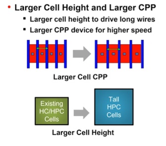
- larger cell height
Wider nFET and pFET devices within a cell provide greater drive strength for the (high-fanout) capacitive loads commonly found in HPC architectures.
- increase in contacted poly pitch (CPP)
A significant parasitic contribution in FinFET devices is the gate-to-source/drain capacitance (Cgd + Cgs) – increasing the CPP increases the cell area (and wire lengths), but reduces this capacitance.
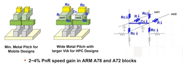
- increased flexibility in back-end-of-line (BEOL) metal pitch (wider wires), with corresponding larger vias, as illustrated below
- high-efficiency metal-insulator-metal (MiM) decoupling capacitor topology
The MiM capacitor cross-section illustrated below depicts three metal “plates” (2 VDD + 1 VSS) for improved areal efficiency over 2-plate implementations.
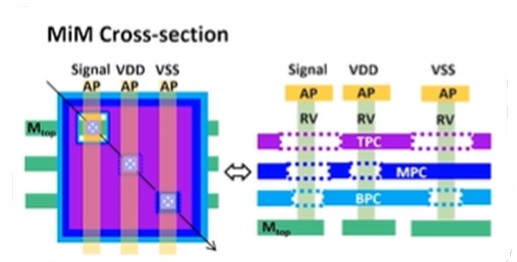
Improved decoupling (and less parasitic Rin to the capacitor) results in less supply voltage “droop” at the switching activity typically found in HPC applications.
- double-height cells
When developing the cell image, the library design team is faced with a tradeoff between cell height and circuit complexity. As mentioned above, a taller cell height allows for more intra-cell wiring tracks to connect complex multi-stage and/or high fan-in logic functions. (The most demanding cell layout is typically a scannable flip-flop.) Yet, a larger cell height used universally throughout the library will be inefficient for many gates.
The DTCO activities for N3HPC led TSMC to adopt a dual-height library design approach. (Although dual-height cells have been selectively employed in earlier technologies, N3HPC adopted more than 400 new cells.) This necessitated extensive collaboration with EDA tool suppliers, to support image techfile definition, valid cell placement rules, and auto-place-and-route algorithms that would successfully integrate single- and double-height cells within the design block. (More on EDA tool features added for N3HPC shortly.)
As part of the N3HPC library design, Y.K. also highlighted that the device sizings in multi-stage cells were re-designed for optimized PPA.
- auto-routing features
Timing-driven routing algorithms have leveraged the reduced R*C/mm characteristics of upper metal layers by “promoting” the layer assignment of critical performance nets. As mentioned above, the N3HPC DTCO efforts have enabled more potential BEOL metal wire lithography width/spacing patterns.
As shown below, routing algorithms needed enhancements to select “non-default rules” (NDRs) for wire width/spacing. (The use of NDRs have been available for quite a while – typically, these performance-critical nets were routed first, or often, manually pre-routed. The N3HPC DTCO features required extending NDR usage as a general auto-route capability.) The figure also depicts how via pillar patterns need to be inserted to support increased signal current.
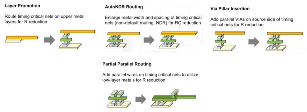
For lower metal layers where the lithography rules are strict and NDRs are not an option, routing algorithms needed to be enhanced to support parallel track routing (and related via insertion), as shown above.
EDA Support
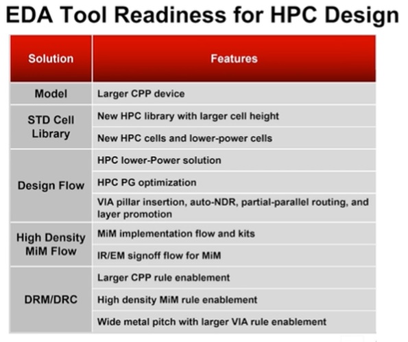
To leverage many of these N3HPC DTCO features, additional EDA tool support was required. The figure below lists the key tool enhancements added by the major EDA vendors.
Summary
TSMC has made a commitment to the high-performance computing platform, to provide significant performance enhancements as part of an HPC-specific process offering. A set of DTCO projects were pursued for N3HPC, providing a cumulative 12% performance gain on a sample Arm core design block. The optimizations spanned a range of design and process lithography window characteristics, from standard cell library design to BEOL interconnect options to MiM capacitor fabrication. Corresponding EDA tool features – especially for auto-place-and-route – have been developed in collaboration with major EDA vendors.
For upcoming process node announcements – e.g., N2 – it will be interesting to see what additional DTCO-driven capabilities are pursued for the HPC offering.
-chipguy
Also read: Highlights of the TSMC Open Innovation Platform Ecosystem Forum
Share this post via:


Comments
One Reply to “Design Technology Co-Optimization for TSMC’s N3HPC Process”
You must register or log in to view/post comments.