The incessant demand for faster data rates across a wide range of end applications has led to the development of the most recent generation of SerDes hardware, achieving 112Gbps. For example, network switches in datacenter architectures are starting to provide 51T throughput utilizing these new 112Gbps implementations (51.2Tbps with 512 lanes).
The 112Gbps SerDes designs will be adopted in a variety of configurations, based on the application. The figure below illustrates Long Reach (LR), Medium Reach (MR), Very Short Reach (VSR), and Extra Short Reach (XSR) topologies, where the 112G signaling path is highlighted in each.
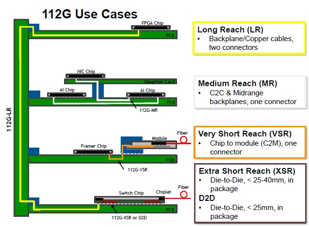
The insertion loss, power per bit, and bit error rate (BER) requirements for these configurations vary considerably – the constraints on the SerDes design to satisfy all these usage cases are considerable.
Yet, there is another consideration to the design of high-speed SerDes IP – namely, the need to support multiple communications protocols, across the gamut of data rates associated with these standards. In other words, the network architect needs the flexibility to program the switch to support legacy data rates within the protocol, as well as enabling the latest generation systems. The figure below provides examples of the multiple protocols and data rates to be supported by a general-purpose high-speed SerDes:
-
- Ethernet
- PCIe
- Common Public Radio Interface (CPRI, between a radio receiver in a tower and a baseband station)
- Fibre Channel.
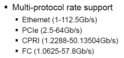
As a result, it is necessary that each lane of the protocol have independent rate programmability with individual speed settings.
At the recent VLSI Symposium on Technology and Circuits, Aida Varzaghani from the High-Speed SerDes design team at Cadence Design Systems presented a thorough description of Cadence’s 112Gbps design, recently fabricated in a 5nm technology node. This article will highlight only a portion of Aida’s presentation, to illustrate the unique clocking design incorporated into the SerDes IP for broadest applicability.
The general architecture of their 112G SerDes is shown in the figure below.
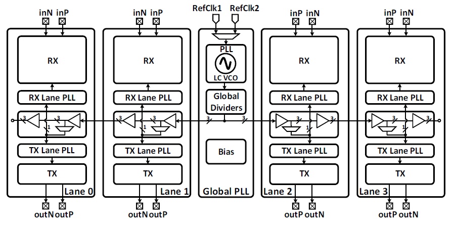
The fundamental macro design is a set of four lanes with an embedded global clock generation unit. (Additional lanes can be added to the macro.) The figure below provides an example of the unique protocol data rates (and signal modulation) that could be programmed for individual lanes sharing the global clock distribution.

As shown in the figure below, the global PLL distributes three (single-ended) clocks to the adjacent Tx/Rx lanes. The table in the figure illustrates examples of the global PLL internal voltage-controlled oscillator (VCO) frequency, and the clocks from the “global dividers” which are output to the lanes. The VCO frequency of the lane PLLs and the final lane clock frequency are also shown.
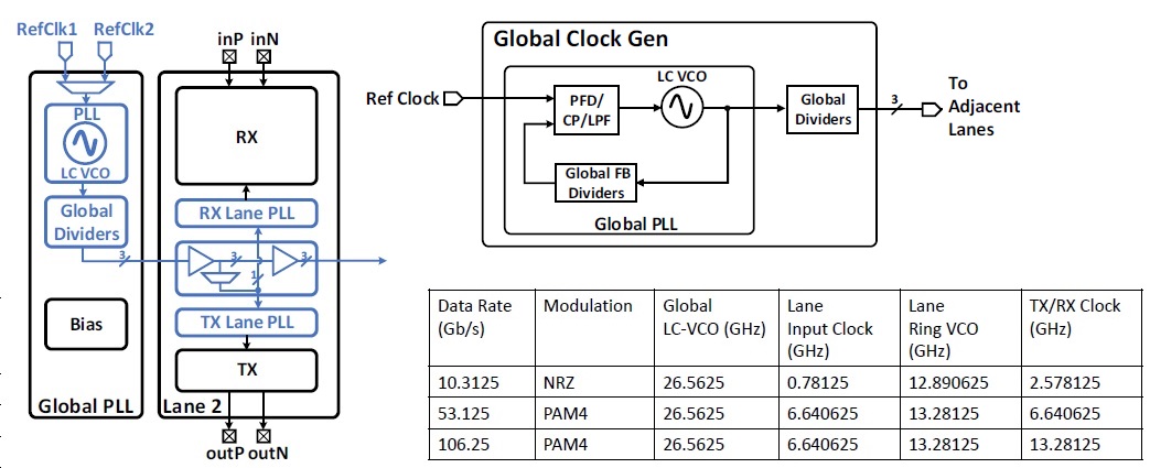
Note that a Tx PLL and an Rx PLL are integrated in each lane. The Tx lane PLL synthesizes the target frequency (at 1/4th of the data rate, as described shortly). The dedicated Rx PLL is used to recover/track the clock from the incoming SerDes data.
The circuitry for the clock input to the lane Tx/Rx PLLs is shown in the figure below.
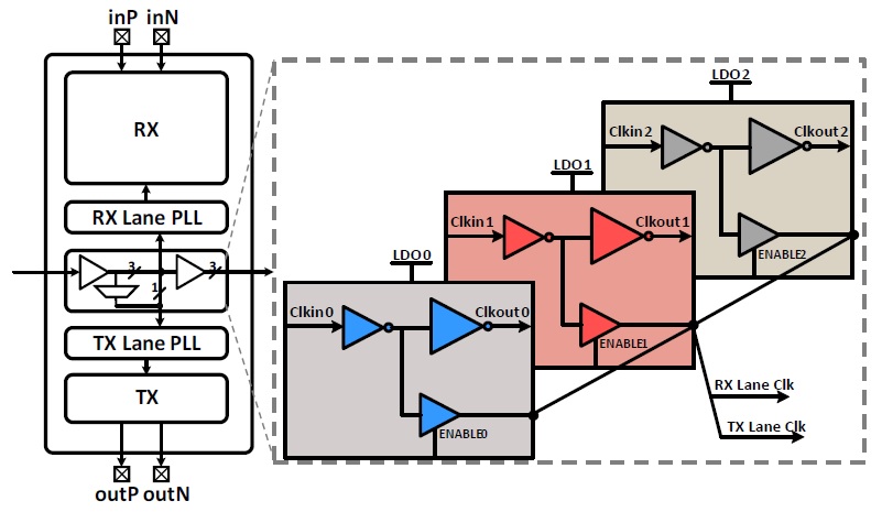
The three input clocks to the lane from the global PLL dividers are multiplexed to the lane PLLs by dotting three driver outputs, with programmable tri-state enables. (A buffer sends the clock to the next lane.) Each driver is sourced by a unique low drop-out regulated supply voltage. This configuration reduces power supply noise-induced jitter in the lane PLL clock input.
The Tx and Rx PLLs are identical, as shown below.
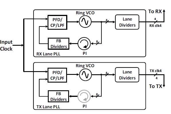
The Ring VCO in each PLL provides four phase-shifted (quadrature) clocks from the base frequency, which defines the unit interval for the data rate transmission, as depicted below.
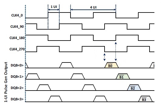
Low data rates are enabled by digital bit stuffing. Aida also presented details on the methods for continuously correcting the duty cycle and minimizing the arrival skews of the (quadrature) clocks to reduce output jitter.
The Rx clock data recovery functionality is supported by a phase interpolator, which adjusts the Rx clock phase to the feedback divider and input phase-frequency detector. The individual phase edges in the interpolator are extracted from the phase-shifted signals within the oscillator, as shown above.
The IP testsite die in the 5nm process node and the loopback test configuration used to characterize the circuitry are shown below.
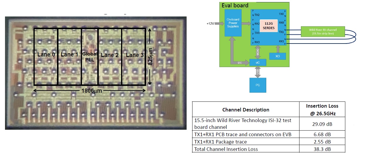
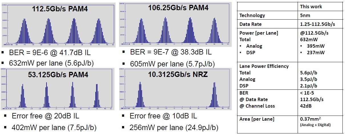
The figure below shows the Rx characteristics from the loopback test – specifically, the power per bit and the BER for different data rates.
Summary
The design of the latest generation high-speed SerDes IP needs to provide maximum flexibility, capable of supporting different protocol standards and a wide range of data rates. Per-lane programmability is an important feature to network architects.
At the recent VLSI Symposium on Technology and Circuits, the Cadence SerDes team recently highlighted their 112G IP macro approach, specifically the unique global and Tx/Rx lane clocking architecture to support these varied protocol and data rate requirements.
For more information on the Cadence 112G SerDes offering, please follow this link.
-chipguy
Also read:
Using AI in EDA for Multidisciplinary Design Analysis and Optimization
Cadence Execs Look to the Future
Stalling to Uncover Timing Bugs. Innovation in Verification
Share this post via:


Comments
There are no comments yet.
You must register or log in to view/post comments.