Everything is becoming digital, and everything digital requires semiconductors. Cadence’s President and CEO, Dr. Anirudh Devgan, highlighted this at the recent CadenceLIVE user conference and discussed many of the company’s accomplishments and future directions. Dr. Devgan also sees the emergence of data—especially unstructured data as another major trend. Such data also affects compute, the cloud, and the edge and is transformational in many ways.
About 45% of Cadence’s customers are system companies that possess both hardware and software and are developing their custom semiconductor solutions. Even traditional semiconductor companies are turning into system companies, as the complexity of their design requires software and system-level hardware to deliver a solution. Mechanical and electrical systems are also converging—mechatronics—and Cadence must ensure it has solutions that cater to the emerging trend. Cadence is partnering with well-established leaders such as Dassault on the mechanical front to link the spheres of mechanical and electronics. As this trend continues, Cadence sees advanced packaging and PCB design playing a more critical role.
Cadence is investing about 40% of its revenue in R&D—one of the largest percentages of any large public company. Cadence has more than 9,500 employees, and more than 8,100 are engineers. As Dr. Devgan stated, the challenge has been to improve productivity and make the design easier to implement, from the transistor level to the cell level to design reuse with intellectual property (IP). One of the tools that the company introduced was the Fidelity CFD software, which provides a streamlined CFD workflow for design, multi-disciplinary analysis, and optimization in a single environment.
The next big frontier will be using AI-based EDA tools to aid in productivity and optimization. A lot of EDA is optimization—place-and-route, layout, and other aspects; however, in the systems space, Cadence wants to ensure the simulation is state of the art; there remains much room in optimization to automate design. At this year’s CadenceLIVE event, Cadence introduced the Optimality Intelligent System Explorer, which delivers very impressive results with its AI-driven multidisciplinary analysis and optimization (MDAO) technology for optimal system design and accuracy. The company also has hardware platforms—Palladium Z2 and Protium X2—that provide a hardware acceleration solution from debug to full software evaluation.
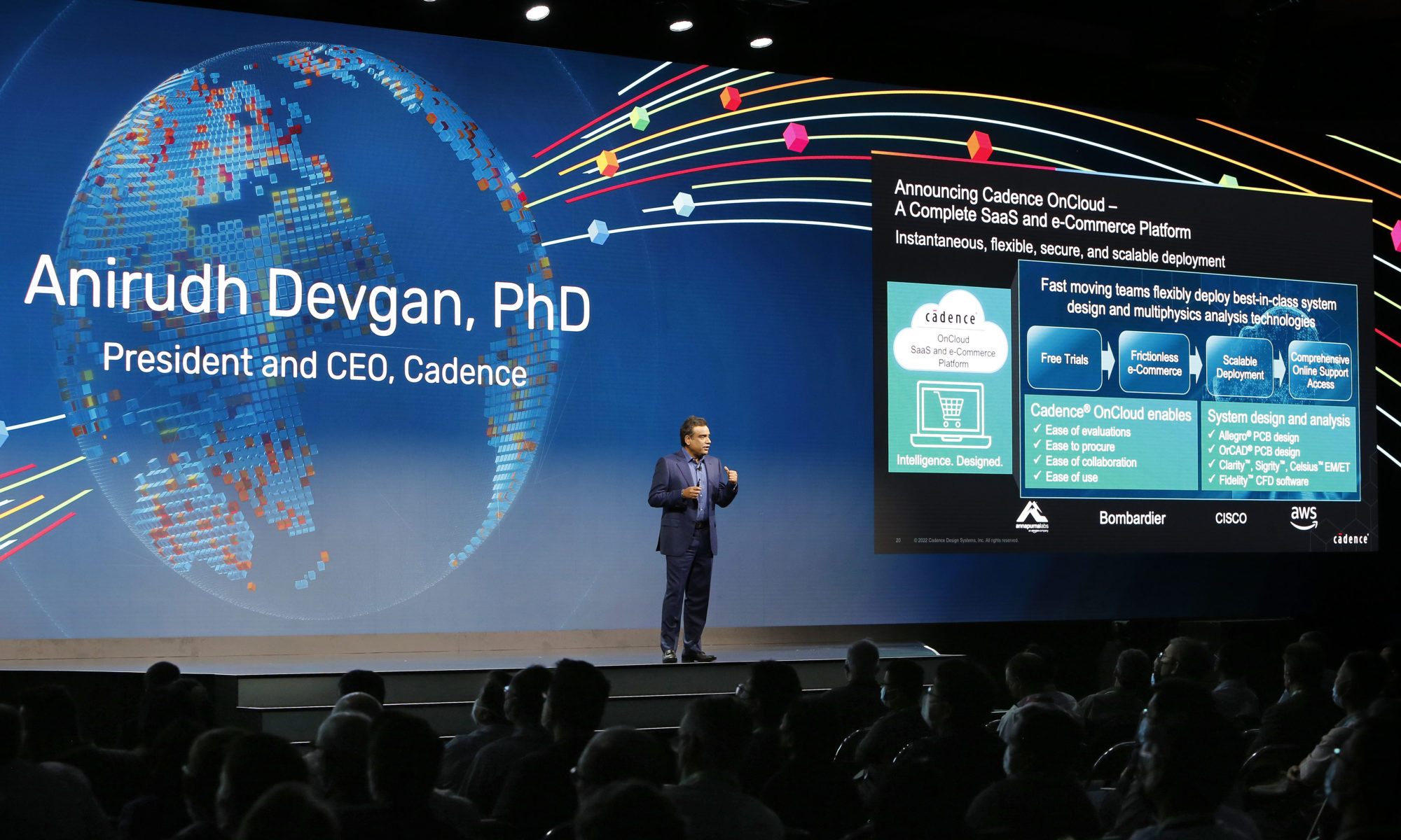
The next step—Cadence OnCloud—a cloud-based design solution where all a designer needs is a web browser to launch Cadence software. It is a flexible consumption-based model with a monthly subscription license and a set number of CPU hours. Designers can purchase more hours as their compute needs increase.

Following Dr. Devgan’s keynote, Tom Beckley, Senior Vice President and General Manager of the Custom IC & PCB Group at Cadence, outlined his group’s tool developments and some future directions. He highlighted the significant increase in the number of mechanical engineers (MEs) that Cadence has hired—about 200 MEs were brought on board to deal with future packaging and thermal design challenges.
Mr. Beckley sees a perfect storm coming in electronics, which is really about the shortage of semiconductors impacting many industries. Additionally, he sees “industry 4.0” unfolding—factories, manufacturing, and delivery are all increasingly electrified, intelligent, and automated. This will result in smart products and an increase in the use of artificial intelligence (AI) and machine learning (ML), which generate large amounts of data.
Over the last few decades, the semiconductor industry has been driven by Moore’s Law, which guided improvements to achieve higher performance, lower power, smaller area, and until recently, lower cost. Additional innovations, roughly grouped as “More-than-Moore,” adds techniques such as new transistor structures, chip stacking, the use of chiplets, and other packaging approaches to improve system integration further. Such packaging approaches also allow the mixing and matching of technologies—optical, RF, high voltage, analog, and digital in a single package.
Cadence is investing heavily in its multiphysics system analysis portfolio. Its solvers are distributed and parallelized, providing higher capacity and performance. The company also enables cross-platform design and analysis for better system optimization. For example, Cadence integrates its Celsius Thermal Solver for package and PCB electrothermal analysis with its Voltus IC Power Integrity Solution, which does IC power integrity signoff so power models can be exchanged in real-time. System heat dissipation always involves both conduction and convection, which is part of the IC package to PCB interface. Finite element analysis can be used to solve the dissipation issues, but then the enclosure and airflow is a fluidics challenge, which is why Cadence is integrating its Fidelity CFD solvers with Voltus and Celsius.
Everything has to be fully modeled and simulated. Cadence has developed several new solutions extending the current Allegro and Virtuoso platforms to support the next generation of wafer-level 3D packaging. The Integrity 3D-IC Platform includes system-level planning, full design, and the company’s analysis, extraction, and verification technologies. Cadence has also partnered with Dassault to connect the Allegro PCB Design software with Dassault’s 3D Experience platform. This transforms the basic electromechanical product development and establishes the first cloud-based end-to-end mechatronic solution. The company has integrated SOLIDWORKS with OrCAD and Allegro to target the mainstream companies.
To handle next-generation RF and millimeter-wave design solutions, tools from Cadence will enable designs in the 30-to-300GHz frequency bands for systems beyond current 5G standards. This will be necessary for the next generation of applications, such as the metaverse, which needs rapid data transmission. Telecom, automotive radar, remote sensing, image security screening, and defense applications will drive the mmWave market with an expected growth of 25% to 30% over the next decade.
Cadence is also partnering with Ericsson on RF and mmWave solutions for complex MIMO antenna arrays and beamforming designs. Such designs demand changes to how RF ICs are designed—the power amplifiers, transceivers, and other circuits. The RF circuits are very sensitive to physical layout, which forces designers to control transmission line widths and lengths during design to achieve the desired impedance values for the circuit. Cadence has integrated Virtuoso for custom ICs with Allegro PCB design to have a single “golden” schematic for RF. The company is also integrating Cadence AWR Microwave Office with Virtuoso Platform, allowing MMIC, TIMIC, and filter designs to move from Microwave Office into Virtuoso for RF SoC design. The SoCs can then move back into Microwave Office for module design or to Allegro for PCB design.
Finally, Mr. Beckley detailed the AI enablement of the Cadence system analysis portfolio. This is expected to deliver a 10X improvement in design productivity plus optimized designs. With the Optimality Explorer, designers can select multiple performance goals to optimize—from the package through to the PCB and back to the package and the chip. With the AI-enabled Optimality Explorer software, designers can allow the software, the cloud, and the processors to do the heavy lifting. All of Cadence’s best-in-class solvers can run on the Optimality engine in parallel. The software can simultaneously address multiple objectives with more than 100 parameters using deep learning technology.
Also read:
Refined Fault Localization through Learning. Innovation in Verification
Tensilica Edge Advances at Linley
Share this post via:


Comments
There are no comments yet.
You must register or log in to view/post comments.