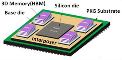
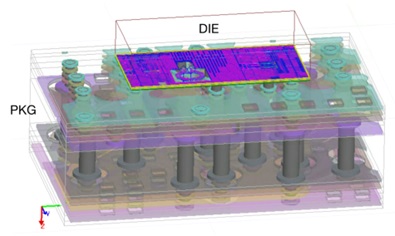
3D-ICs bring together multiple silicon dies into a single package that’s significantly larger and complex than traditional systems on a chip (SoCs). There’s no doubt these innovative designs are revolutionizing the semiconductor industry.
3D-ICs offer a variety of performance advantages over traditional SoCs. Because of their integrated, stacked design, they eliminate the reticle limits that define the maximum size of a single die. They deliver faster signal speeds with lower power consumption requirements. Stacking memory chiplets directly on top of logic minimizes delays. 3D-ICs enable design innovation, by allowing a combination of different silicon process technologies to be applied in a single integrated system.
With their potential for lower power, greater integration density, and faster data rates, 3D-ICs are poised to help deliver on the promise of 5G and 6G networks, the Industrial Internet of Things (IIoT), product autonomy, vehicle electrification, and other emerging technology trends. Based on the degree to which they can outperform any single chip, 3D-ICs represent the future of the global semiconductor industry.
But is your team prepared for that future? Along with their significant benefits, 3D-ICs deliver some daunting challenges for product development organizations that have built their success on single-die designs.
Changing IC Design: The Cultural Impact
One of the biggest challenges is cultural. As 3D-ICs revolutionize the marketplace, they’re also quietly revolutionizing foundational product development processes across the worldwide semiconductor industry.
The 3D-IC revolution is blurring the lines between system and silicon, as three traditionally separate design disciplines — chip design, package design, and board design — are now merging. Successfully designing and fabricating a 3D-IC requires significant synergy between all three disciplines.
As design spans multiple dies, the packaging of these chips becomes an integral part of a larger system, which means that chip and package designers must optimize their solutions collaboratively and simultaneously. For example, as logic blocks are dispersed across two or more dies, they communicate through wiring positioned in the package substrate or interposer layer — merging package design with the floorplanning of the chip. Chiplets stacked vertically on top of other chiplets, and connected through direct microbump contacts, further blur the lines between package and die. The interconnect routing on a large 3D-IC substrate — which is a complex mixture of chip and board strategies like non-Manhattan routing, river routing, and electromagnetic modeling — also demands a crossfunctional, concurrent design approach.


The complex, stacked design of 3D-ICs continues to blur the lines between silicon and system. As the packaging of each individual chip becomes part of a larger system, chip, board, and package designers must work together collaboratively and concurrently to optimize overall product performance. The Ansys simulation platform is built to manage this type of multiphysics, interdisciplinary engineering analysis, delivering best-in-class physics capabilities along with seamless workflows and design automation.
While every company’s process for managing these complex engineering problems is different, the easy separation between chip, package, and board is now being definitively erased.
The problem? Suddenly it’s unclear who is responsible for what, and who is accountable for the ultimate success of a given 3D-IC design. Whose priorities are more important? Who gives the final signoff? And how exactly should cross functional collaboration happen? In many organizations, entirely new competencies and roles are being added to the traditional product design team. Even more challenging, today, those groups typically don’t even exist in the same company.
In the new 3D-ICs world , cross functional and interdisciplinary experts now need to work together as a close-knit team that actively collaborates on every aspect of design on a daily basis. Together, they need to optimize the board, the package, and the silicon simultaneously. Functional silos and a serial design process, characterized by handoffs among disciplines, must be replaced by cohesion, concurrent design, and teamwork.
Equally Important? The Technology Impact
How can semiconductor manufacturers support this new level of collaboration? A key requirement is to address their second big challenge: embracing of new technology approaches that are purpose-built for the kind of concurrent, system-level design required by 3D-ICs. Today product development teams not only need to optimize designs at the system level — considering component interactions and connection points — but they also need to consider novel physics that they’ve never analyzed before.
As just one example, power dissipation is a primary constraint in 3D-IC design, and optimizing this performance aspect requires a true multiphysics approach. Mechanical analysis, including modeling the stress and warpage of the package, must be considered from the earliest stage. It must be analyzed concurrently with floorplanning because the suboptimal placement of hot and not-so-hot components can have disastrous implications for stress, warpage, and ultimate power dissipation. Another novel, multivariate challenge is the crossfunctional analysis required to eliminate low-frequency power supply oscillations between components on the substrate.
Traditional single-physics simulation tools, applied by different functions in a serial approach, are simply not up to the challenge of 3D-IC design.
. In today’s fast-paced, hypercompetitive environment, neither option supports success.
The Ansys Platform: A New Approach
There is good news. Ansys has developed a purpose-built platform for collaborative and concurrent 3D-IC design. The Ansys platform is a modern concept, built for the 3D-IC .
Backed by 50 years of industry leadership, Ansys delivers gold-standard revolution simulation solutions necessary for designing an optimal 3D-IC design. These include power integrity, reliability, electromagnetics (EM), thermal, computational fluid dynamics (CFD) and mechanical analyses. Now Ansys delivers these capabilities via an open, flexible, extensible, and high-capacity design platform that enables product development teams to subject the entire 3D-IC design to real-world operating parameters and simultaneously optimize the multiple physics.
While large, well-resourced corporations benefit from a vertically integrated culture that enables interdisciplinary collaboration — and they can more easily introduce bespoke silicon designs — smaller, more horizontally integrated companies may struggle to achieve the level of teamwork and crossfunctional collaboration needed to optimize 3D-ICs.
By leveraging the unified Ansys platform, every product development team can easily collaborate across functions in a shared, multiphysics design ecosystem. Design automation, synergistic workflows, and a best-in-class multiphysics portfolio from Ansys support 3D-IC innovation and speed new designs to market, without sacrificing analytic rigor.
The Ansys platform enables multiple physical effects, multiple integration points, and system-level performance to be considered quickly and cost-effectively. It encapsulates and delivers the required expertise, including novel physics, in an intuitive, easy-to-use solution that’s accessible to the entire cross functional design team.
As the lines continue to blur between silicon and system, Ansys helps to make these challenges manageable, focusing on fast, easy component and system-level analysis and verification.
Learn More About the Ansys Platform at DAC 2022
Want to adopt a revolutionary new design approach that positions you for leadership in the 3D-IC revolution? Learn more by visiting Ansys at Booth #1539 at the upcoming Design Automation Conference (DAC), held in San Francisco July 10-14. Request a meeting or product demo now and prepare for success in today’s new environment of blurred lines and concurrent design. Reserve your space for Ansys’ DAC Breakfast event, 3D-IC Design in a 2D World cohosted with Synopsys, and moderated by yours truly.
Also Read:
Multiphysics, Multivariate Analysis: An Imperative for Today’s 3D-IC Designs
A Different Perspective: Ansys’ View on the Central Issues Driving EDA Today
Unlock first-time-right complex photonic integrated circuits
Share this post via:


Comments
4 Replies to “The Lines Are Blurring Between System and Silicon. You’re Not Ready.”
You must register or log in to view/post comments.