You are currently viewing SemiWiki as a guest which gives you limited access to the site. To view blog comments and experience other SemiWiki features you must be a registered member. Registration is fast, simple, and absolutely free so please,
join our community today!
In an era dominated by artificial intelligence (AI), machine learning (ML), and high-performance computing (HPC), the demand for semiconductors that deliver high data throughput, low latency, and energy efficiency has never been greater. Traditional chip designs often struggle to keep pace with these requirements, leading… Read More
Traditional methods of chip design and packaging are running out of steam to fulfill growing demands for lower power, faster data rates, and higher integration density. Designers across many industries – like 5G, AI/ML, autonomous vehicles, and high-performance computing – are striving to adopt 3D semiconductor… Read More
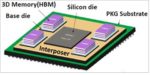
3D-ICs bring together multiple silicon dies into a single package that’s significantly larger and complex than traditional systems on a chip (SoCs). There’s no doubt these innovative designs are revolutionizing the semiconductor industry.
3D-ICs offer a variety of performance advantages over traditional SoCs. Because … Read More
Summary
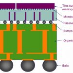
Thermo-compression bonding is used in heterogeneous 3D packaging technology – this attach method was applied to the assembly of large (12-stack and 16-stack) high bandwidth memory (HBM) die, with significant bandwidth and power improvements over traditional microbump attach.
Introduction
The rapid growth of heterogeneous… Read More
Have you ever had the experience where you look up some unusual word in the dictionary since you don’t remember seeing it before. And then, in the next few weeks you keep coming across it. Twice in the last week I have been in presentations about the economics of putting die onto silicon interposers and the possibility of a new… Read More