You are currently viewing SemiWiki as a guest which gives you limited access to the site. To view blog comments and experience other SemiWiki features you must be a registered member. Registration is fast, simple, and absolutely free so please,
join our community today!
Contrary to the popular press, ASML High-NA EUV is not ready for logic production yet—and it may never be, at least not in the form originally envisioned. If you remember how long it took conventional EUV to become production-worthy—arguably 5–10 years—this should not come as a surprise. More importantly, this is no longer just… Read More
The imec installation of the ASML EXE:5200 High Numerical Aperture (High NA) extreme ultraviolet (EUV) lithography system at imec represents a pivotal advancement in semiconductor manufacturing and research. This system, installed in imec’s 300 mm cleanroom in Leuven, Belgium, introduces unprecedented lithographic resolution… Read More
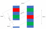
For the so-called “2nm” node or beyond, the minimum metal pitch is expected to be 20 nm or even less, while at the same time, contacted gate pitch is being pushed to 40 nm [1]. Therefore, we expect via connections that can possibly be as narrow as 10 nm (Figure 1)! For this reason, it is natural to expect High-NA EUV lithography as the go-to
…
Read More
In High-NA EUV lithography systems, the numerical aperture (NA) is expanded from 0.33 to 0.55. This change has been marketed as allowing multi-patterning on the 0.33 NA EUV systems to be avoided. Only very recently have specific examples of this been provided [1]. In fact, it can be shown that double patterning has been implemented… Read More
Dinesh Bettadapur serves as the Chief Executive Officer of Irresistible Materials Ltd. Dinesh has over 20 years of executive management experience in the semiconductor industries and has held significant leadership roles encompassing general management, P&L management, sales, business development, strategic alliances,… Read More
Whether EUV or DUV doesn’t matter at 20 nm pitch
The International Roadmap for Devices and Systems, 2022 Edition, indicates that the “2nm” node due in 2025 (this year) has a minimum (metal) half-pitch of 10 nm [1]. This is, in fact, less than the resolution of a current state-of-the-art EUV system, with a numerical aperture… Read More
- News reports that Trump will change CHIPS Act to suit his views
- We specifically predicted this months ago as deals closed 11th hour
- Blue states, enemies list & foreign entities likely to get cut
- Big changes/cuts likely to a program Trump roundly criticized
Reuters: Exclusive: Trump prepares to change US CHIPS Act conditions,… Read More
On Friday April 12th Intel held a press briefing on their adoption of High NA EUV with Intel fellow and director of lithography Mark Phillips.
In 1976 Intel built Fab 4 in Oregon, the first Intel fab outside of California. With the introduction of 300mm Oregon became the only development site for Intel with large manufacturing, development,… Read More
ASML- better EPS but weaker revenues- 2024 recovery on track
China jumps 10% to 49%- Memory looking better @59% of orders
Order lumpiness increases with ASP- EUV will be up-DUV down
“Passing Bottom” of what has been a long down cycle
Weak revenues & orders but OK EPS
Reported revenue was Euro5.3B and EPS of Euro3.11… Read More
– High NA EUV’s coming out party – “Dawn” of the Angstrom Era
– Well attended, positive vibes, not much new but good progress
– Concerns about Samsung slowing spend while Intel accelerates
– KLA reticle inspection quandary – Risky business in China
SPIE was a High-NA
…
Read More