

There has been much interest in Huawei’s and SMIC’s plans for 5nm production in the near future. Since there is no use of EUV in China, immersion DUV lithography (with a 76 nm pitch resolution) is expected to be used along with pitch quartering to achieve pitches in the 20-30 nm range expected for the 5nm and 3nm nodes [1].
However, Samsung and TSMC were early adopters of EUV technology, and had not demonstrated the use of immersion lithography with pitch quartering in their metal layers, for 7nm onwards. Intel used pitch quartering with an extended effort to bring 10nm (now Intel 7) to production. This effort spanned years, with Intel subsequently adopting EUV. One thing in common with all these 7nm developments was that they all had been disclosed in the 2017-2018 timeframe. Hence, all three companies have not had the chance to digest the latest improvements in multipatterning productivity at the time. In this article, we will cover how these developments can be used to eliminate the expected burden of multipatterning involving pitch quartering, as expected for 7nm, 5nm, and 3nm nodes.
Self-Aligned Blocks
The first key development to highlight is the use of self-aligned blocking. This was published in 2017 [2-4]. The motivation here is that in order to cut lines with pitches between 20 and 40 nm into interconnect patterns, many (4 or more) additional block masks would be needed [2]. Moreover, the tight placement control for the individual patterns for blocking the trench etch due to rounding [5] is still thwarted by stochastic behavior. To alleviate this, self-aligned blocking arranges the lines to be alternately divided into two groups, each consisting of a different material to be etched (Figure 1). The two materials may be silicon dioxide and silicon nitride, for example. This division into two etch material groups naturally occurs with pitch quartering by self-aligned quadruple patterning (SAQP) [2].

Figure 1. Self-aligned blocking scheme. Left: original block arrangement has four separate cut masks (each indicated by different color). Right: self-aligned blocking allows two cut masks for the block arrangement.
By ensuring that the adjacent line material is not etched, the blocking pattern can be elongated, merging aligned cuts on every other line, as well as circumventing rounding consequences. As shown in Figure 1, four cut masks can be reduced to two. As EUV also needs to avoid the effects of stochastic rounding and edge placement error, self-aligned blocking has been incorporated into the well-known SALELE scheme [6].
Block/Cut Redistribution/Expansion
The second key development to highlight was disclosed even earlier [7-9]. The idea here is to redistribute cut locations by extending and/or shifting line segments (wires) as needed. Figure 2 shows an M0 (lowest metal layer) example [8].
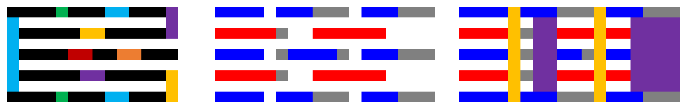
Figure 2. Left: Original M0 layout requiring six cut masks. Center: Wire shifts and extension applied. Right: Self-aligned blocking applied, resulting in only two cut masks.
The extension and shifting of wires is effectively imposing a lower limit on wire length, allowing the minimization of cut mask cost, becoming two cut masks for either DUV or EUV case. Wire lengths going lower than this limit would entail two cut masks per etch material. Note that a single cut mask exposure using EUV is still at least 20% more expensive than two exposures using DUV [10-12]. Also, the cost of two EUV exposures for generating sub-40 nm pitch lines is more than 30% higher than that of SAQP with a single DUV immersion exposure [10,13].
For the longer lines on higher metal layers, like M2, the extra capacitance from extending the lines can be a concern [9]. An alternative to the cut approach may be letting the lines stagger with extended gaps between line ends (Figure 3) [9].
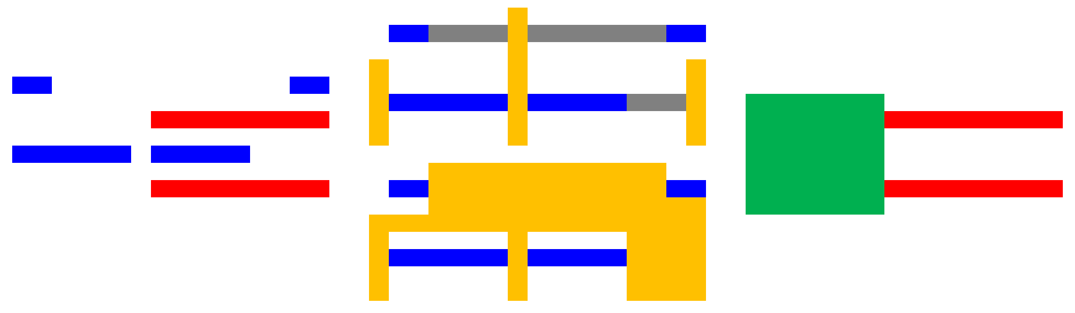
Figure 3. Left: M2 lines with assigned etch material in different colors. Center top: line extension applied for blue cut distribution. Center bottom: Without extension, an expanded block is used. Right: Expanded block for red cut.
The line end gaps are naturally filled by expanding the block patterns instead of extending the affected lines. Perhaps the final shapes of the expanded block patterns can be fine-tuned by computational lithography such as NVIDIA’s cuLitho.
Vias in Self-Aligned Blocking Scheme
As a third key development, the patterning of self-aligned vias [14] in the self-aligned blocking scheme should follow the splitting into two etch materials, and can also take advantage of the doubling of the etch mask pitch (Figure 4). This leads to two via lithography masks corresponding to the two etch materials.

Figure 4. Self-aligned via with self-aligned blocking. Left: Block mask (green) for red etch material. Center left: Via photoresist mask (gray) for red etch material. Center right: Partial etch for via (brown) in red etch material, and removal of via mask. Right: Removal of block mask, revealing previously patterned blue etch material and via.
What If…?
If the start of 7nm development happened after 2017, most likely DUV immersion lithography would have been used not with brute-force multipatterning but with self-aligned blocking and block redistribution / expansion. There would be a maximum of two cut masks per metal layer (with an additional two in worst case for M0) and two masks per via layer (with an additional two in worst case for V0), corresponding to the two etch materials.
Once in use, the 5nm and 3nm nodes would also have been covered. EUV development would of course still be continuing to keep pace, and perhaps the NA would have been increased earlier. It would have been an interesting alternative history but now, going forward, it appears only new semiconductor players at advanced nodes can exploit the full benefit of 20-20 hindsight.
References
[1] F. Chen, 2023 https://www.linkedin.com/pulse/extension-duv-multipatterning-toward-3nm-frederick-chen
[2] F. Lazzarino et al., Proc. SPIE 10149, 1014908 (2017)
[3] A. Raley et al., Proc. SPIE 10149, 101490O (2017).
[4] Y. Chen, US Patent 9679771.
[5] W. Gao et al., Proc. SPIE 9426, 942606 (2015).
[6] Y. Drissi et al., Proc. SPIE 10962, 109620V (2019).
[7] Z. Xiao et al., Proc. SPIE 8880, 888017 (2013).
[8] S. Sakhare et al., Proc. SPIE 9427, 94270O (2015).
[9] W. Gillijns et al., Proc. SPIE 9427, 942709 (2015).
[10] L. Liebmann et al., Proc. SPIE 9427, 942702 (2015).
[11] S. Snyder et al., 2021 EUVL Workshop, https://www.euvlitho.com/2021/P2.pdf
[12] J. van Schoot et al., 2021 https://conference-indico.kek.jp/event/125/contributions/2304/attachments/1711/1951/Presentation_Jan_van_Schoot_et_al.ASML.pdf
[13] L-A. Ragnarsson et al., “The Environmental Impact of CMOS Logic Technologies,” 2022 EDTM.
[14] J-H. Franke et al., Proc. SPIE 10145, 1014529 (2017).
This article first appeared in LinkedIn Pulse: Self-Aligned Block Redistribution and Expansion for Improving Multipatterning Productivity
Also Read:
ASML- Soft revenues & Orders – But…China 49% – Memory Improving
TSMC and Synopsys Bring Breakthrough NVIDIA Computational Lithography Platform to Production
Measuring Local EUV Resist Blur with Machine Learning
Share this post via:


Podcast EP357: How Gonka is Changing the Way AI is Accessed with David Liberman