Resist blur remains a topic that is relatively unexplored in lithography. Blur has the effect of reducing the difference between the maximum and minimum doses in the local region containing the feature. Blur is particularly important for EUV lithography since EUV lithography is prone to stochastic fluctuations and also driven by secondary electron migration, which presents a significant source of blur [1].
While optical sources of blur, such as defocus, flare, and EUV dipole image fading [2], can be considered as independent of wafer location, non-optical sources, such as from electron migration or acid diffusion, can have a locally varying behavior. It is therefore important to have some way to characterize and/or monitor the local blur in a patterned EUV resist.
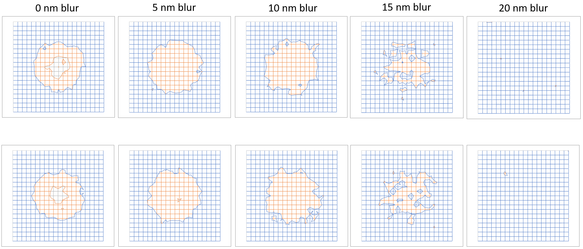
The most straightforward way is to have a resist pattern that covers the whole exposure field with adequate resolution-scale sampling. A practical choice for a 0.33 NA EUV system would be a 20 nm half-pitch hole or pillar array, which gives equal sampling in x and y directions. It is also practically at the resolution limit for contact/via patterning due to stochastic variations [3,4]. As shown for an example in Figure 1, a large enough blur, e.g., 20 nm, is enough for the contact to go missing. Such a large blur may result from local resist inhomogeneities as well as occasionally large electron range.

Figure 1. 20 nm half-pitch via pattern, at 20 mJ/cm2 absorbed dose (averaged over 40 nm x 40 nm cell), with different values of blur. Quadrupole illumination is used with a darkfield mask. Secondary electron quantum yield = 2. A Gaussian was fit to the half-pitch via.
One can envisage that machine learning methods [5] can be used to match via appearance to the most likely blur at a given location, allowing a blur map to be generated for the whole exposure field. It also should be reminded that the rare large local blur scenario is consistent with the rare occurrence of stochastic defects [6]. Thus, studying local blur is important for basic understanding of not just the resist but also of the origin of stochastic defects.
References
[1] P. Theofanis et al., Proc. SPIE 11323, 113230I (2020).
[2] J-H. Franke, T. A. Brunner, and E. Hendrickx, J. Micro/Nanopattern. Mater. Metrol. 21, 030501 (2022).
[3] W. Gao et al., Proc. SPIE 11323, 113231L (2020).
[4] F. Chen, “Via Shape Stochastic Variation in EUV Lithography,” https://www.youtube.com/watch?v=Cj1gfDV7-GE
[5] C. Bishop, Pattern Recognition and Machine Learning, https://www.microsoft.com/en-us/research/publication/pattern-recognition-machine-learning/
[6] F. Chen, “EUV Stochastic Defects from Secondary Electron Blur Increasing with Dose,” https://www.youtube.com/watch?v=Q169SHHRvXE, “Modeling EUV Stochastic Defects with Secondary Electron Blur,” https://www.linkedin.com/pulse/modeling-euv-stochastic-defects-secondary-electron-blur-chen
This article first appeared in LinkedIn Pulse: Measuring Local EUV Resist Blur with Machine Learning
Also Read:
Pinning Down an EUV Resist’s Resolution vs. Throughput
Application-Specific Lithography: Avoiding
Stochastic Defects and Image Imbalance in 6-Track Cells
Share this post via:


The Semiconductor Growth Numbers are Insane but the Real World Doesn’t Tally!