You are currently viewing SemiWiki as a guest which gives you limited access to the site. To view blog comments and experience other SemiWiki features you must be a registered member. Registration is fast, simple, and absolutely free so please,
join our community today!
Earlier this month, TechInsights did a teardown of the Kirin 9030 chip found in Huawei’s Mate 80 Pro Max [1]. Two clear statements were made on the findings: (1) the transistor density of SMIC’s “N+3” process was definitely below that of the earlier 5nm processes from Samsung and TSMC, and (2) metal pitch was aggressively scaled
…
Read More
For the so-called “2nm” node or beyond, the minimum metal pitch is expected to be 20 nm or even less, while at the same time, contacted gate pitch is being pushed to 40 nm [1]. Therefore, we expect via connections that can possibly be as narrow as 10 nm (Figure 1)! For this reason, it is natural to expect High-NA EUV lithography as the go-to
…
Read More
Whether EUV or DUV doesn’t matter at 20 nm pitch
The International Roadmap for Devices and Systems, 2022 Edition, indicates that the “2nm” node due in 2025 (this year) has a minimum (metal) half-pitch of 10 nm [1]. This is, in fact, less than the resolution of a current state-of-the-art EUV system, with a numerical aperture… Read More
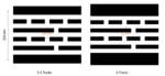
At IEDM 2019, TSMC revealed two versions of 5nm standard cell layouts: a 5.5-track DUV-patterned version and a 6-track EUV-patterned version [1]. Although the metal pitches were not explicitly stated, later analyses of a 5nm product, namely, Apple’s A15 Bionic chip, revealed a cell height of 210 nm [2]. For the 6-track … Read More
In recent advanced nodes, via and cut patterning have constituted a larger and larger portion of the overall BEOL mask count. The advent of SALELE [1,2] caused mask count to increase for EUV as well, resulting in costs no longer being competitive with DUV down to 3nm [3]. Further development by TEL [4] has shown the possibility for… Read More
China’s recent achievement of a 7nm-class foundry node using only DUV lithography [1] raises the question of how far DUV lithography can be extended by multipatterning. A recent publication at CSTIC 2023 indicates that Chinese groups are currently looking at extension of DUV-based multipatterning to 5nm, going so far… Read More
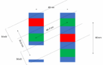
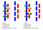
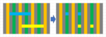
The 5nm foundry node saw the arrival of 6-track standard cells with four narrow routing tracks between wide power/ground rails (Figure 1a), with minimum pitches of around 30 nm [1]. The routing tracks require cuts [2] with widths comparable to the minimum half-pitch, to enable the via connections to the next metal layer with the… Read More
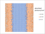
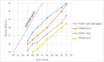
Ongoing investigations of EUV stochastics [1-3] have allowed us to map combinations of critical dimension (CD) and pitch which are expected to pose a severe risk of stochastic defects impacting the use of EUV lithography. Figure 1 shows a typical set of contours of fixed PNOK (i.e., the probability of a feature being Not OK due… Read More
Toshiba (now known as Kioxia) was the first company to propose a 3D stacked version of NAND Flash memory called BICS [1]. BICS (BIt Cost Scalable) Flash used explicit process cost reduction based on depositing and etching multiple layers at once, avoiding multiple lithography steps. This strategy replaced the usual approach… Read More
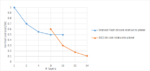
Nonvolatile memory capacity reached 64 Gb levels when NAND Flash half-pitch reached 20 nm [1]. Having reached 14 nm [2], NAND Flash half-pitch is no longer being reduced, now that it has entered the 3D era. However, recently, 3D XPoint has found applications within the Optane platform [3]. The lithography for patterning 20 nm half-pitch… Read More