

In a previous article [1], the Rayleigh criterion was mentioned as the resolution limit for the distance between two features. On the other hand, in a following article [2], the minimum pitch was mentioned for the resolution limit for arrayed features. In this article, we reconcile the two by considering gaps between arrayed features, for example, between a minimum pitch line end and the edge of a perpendicular line.
Counting Spatial Harmonics (Diffraction Orders)
The number of features that can fit into the pitch equals the number of spatial harmonic intervals (=wavelength/pitch) that are passed by the numerical aperture (NA) of the optical system. If 5 spatial harmonics, or diffraction orders beyond the zeroth, are passed, then five intensity peaks emerge, indicating a minimum feature size of one-fifth the pitch (Figure 1).

Figure 1. The fundamental (1st harmonic) only generates one feature per pitch, while the fifth harmonic generates five.
With a minimum pitch of wavelength/NA in the horizontal direction, and a wider pitch in the vertical direction, the number of features spaced vertically within the vertical pitch at most will be the number of diffraction orders in the vertical direction (besides the zeroth), and this will depend on the illumination. The minimum pitch dictates an optimum illumination (e.g., dipole or quadrupole) which will limit the number of diffraction orders to two in the horizontal direction and a given number in the vertical direction. By dividing the vertical pitch by the number of diffraction order intervals, the minimum gap in the vertically running line can be estimated (Figure 2).

Figure 2. Left: The optimum illumination for a given pitch between vertical lines will arrange to have the diffraction orders at equal horizontal distances from the center, while allowing a number to spread out vertically. The circle represents the numerical aperture which will cut off diffraction orders which fall outside. Center: Top view of aerial image of a rectangle between horizontal lines. The cut line aerial image (right) from the center cutline shows the gap where intensity drops is roughly 1/5 the vertical pitch, as expected from the number of included diffraction order intervals.
This is calculated for a range of minimum pitches and cross-pitches and plotted in Figure 3.

Figure 3. Left: Tip-to-edge gap for a line pitch of wavelength/NA, as a function of cross-pitch, normalized to wavelength/NA. Right: Tip-to-edge gap for a cross-pitch of 4 x line pitch, as a function of line pitch, normalized to wavelength/NA. The illumination is optimized for the line pitch.
In fact, the lower limit of gap size can be calculated exactly if the minimum line pitch is at most wavelength/NA. It is sqrt(3)/3 * wavelength/NA. The proof is given in the Appendix.
Sanity Check: consistency with the Rayleigh Criterion
The Rayleigh criterion and the arrayed feature results are both derived from Fourier transforms truncated by the numerical aperture. The Airy disc underlying the Rayleigh criterion comes from the Fourier transform of a circular aperture while the Fourier transform of an array produces a Fourier series convolved with the apertures within a pitch. Hence, there should be no conflict between the above and previous [2] arrayed feature results and the Rayleigh criterion.
Shrinking the gap below k1=0.6
An interesting effect is predicted when the gap is smaller than 0.6 wavelength/NA. It appears as if less light is absorbed or transmitted (reflected for EUV case) by the shrinking feature. This can lead to resist scumming for example [4]. This can be understood by considering the amplitudes of the harmonics (Figure 4).

Figure 4. The amplitudes of the spatial harmonics (diffraction orders) which are not cut off by the numerical aperture all decrease when the gap size falls below 0.6 wavelength/NA (k1=0.6), but above this size, the higher harmonics decrease while the lower ones increase.
For features below 0.5-0.6 wavelength/NA, the amplitudes of all the harmonics decrease with decreasing size. However, for features sized 0.6 wavelength/NA and higher, the higher harmonic amplitudes decrease as size is increased while the lower harmonics have the opposite trend, indicating a trend toward sharper edges [5]. Below 0.6 wavelength/NA, gaps in lines are better patterned by a separate cut mask exposure [6]. This allows the smaller line end gaps to be compensated with a higher dose.
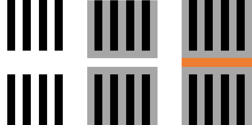
The gap between line end and perpendicular line edge can also be reduced below ~0.6 wavelength/NA by spacer patterning within an initially wider starting gap (Figure 5). This approach is also known as spacer-is-dielectric self-aligned double patterning (SID SADP) [7].

Figure 5. SID SADP approach to reducing gap width.
Summary of Lithography Resolution Limits
The lithography resolution limits are now summarized as follows:
Gap between isolated pairs: 0.61 wavelength/NA
Minimum pitch of arrayed features: 0.5 wavelength/NA/(1-angle tolerance)
Line end gaps for line pitch<=wavelength/NA: 0.58 wavelength/NA
Appendix: Derivation of lower limit of arrayed gap size for minimum line pitch of wavelength/NA or less
The starting point here is that for a minimum pitch p <= wavelength/NA (dense line k1<=0.5), the illumination will first produce the diffraction order distribution shown on the left in Figure 2. In terms of spatial frequency coordinates, this means the x-coordinates are +/- 0.5 wavelength/p. Here we express the y-pitch as a multiple of the minimum pitch, i.e., np. The diffraction order interval is therefore wavelength/p/n. The number of such intervals which fit within the numerical aperture NA is therefore given by
N=2 * sqrt(NA^2-(0.5 wavelength/p)^2)/(wavelength/p/n)
= 2 n sqrt((p*NA/wavelength)^2-1/4). (1)
The estimated gap size is therefore
gap size = np/N = n p/ [2 n sqrt((p*NA/wavelength)^2-1/4)]
= p/sqrt[(2 NA p/wavelength)^2-1]. (2)
Since p lies within the range 0.5-1 wavelength/NA, the minimum gap size occurs for p = wavelength/NA, giving a gap size of 1/sqrt(3) wavelength/NA = sqrt(3)/3 wavelength/NA ~ 0.58 wavelength/NA (Figure 6). Note that this is larger than the nominal line spacing (k1<=0.5). So, for connections to the next layer that must not exceed k1=0.5, the gap must be printed with a cut mask.

Figure 6. Gap size vs. line pitch, where both are normalized to wavelength/NA (k1=dimension/(wavelength/NA)).
References
[1] https://www.linkedin.com/pulse/lithography-resolution-limits-paired-features-frederick-chen/
[2] https://www.linkedin.com/pulse/lithography-resolution-limits-arrayed-features-frederick-chen/
[3] https://en.wikipedia.org/wiki/Fourier_optics
[4] D. Chou, K. McAllister, “Line end optimization through optical proximity correction (OPC): a case study,” Proc. SPIE 6154, 61543A (2006).
[5] https://user.eng.umd.edu/~tretter/enee322/FourierSeries.pdf
[6] Z. Li et al., “The study of 28nm node poly double patterning integrated process,” CSTIC 2015.
[7] Y. Du et al., “Enhanced spacer-is-dielectric (sid) decomposition flow with model-based verification,” Proc. SPIE 8684, 86840D (2013).


TSMC CoWoS versus Intel EMIB Semiconductor Packaging