

Nonvolatile memory capacity reached 64 Gb levels when NAND Flash half-pitch reached 20 nm [1]. Having reached 14 nm [2], NAND Flash half-pitch is no longer being reduced, now that it has entered the 3D era. However, recently, 3D XPoint has found applications within the Optane platform [3]. The lithography for patterning 20 nm half-pitch lines that make up these memories is another opportunity to look at basic aspects and limitations of currently known lithographic approaches in the industry.
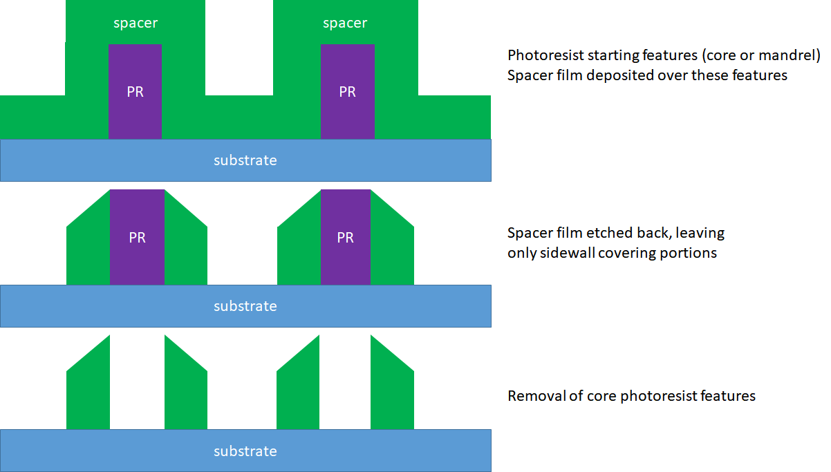
The method for patterning 20 nm half-pitch lines is self-aligned double patterning (SADP). This approach starts with 80 nm pitch lines which actually only serve to support sidewall layers known as spacers (Figure 1). Etching the spacers vertically leaves only the sidewall portions. The original lines are then removed, and the spacers form a 40 nm pitch line pattern.

Figure 1. With SADP (self-aligned double patterning), sidewall spacers define twice as many lines as the starting photoresist.
With SADP, the feature dimension is determined by the spacer width, which, in turn, is controlled by deposition. The lithography does not affect the feature dimension, but an error could produce alternate spacing errors (“pitch walking”); this may be compensated by having the lithography synchronized with subsequent spacer deposition and etching [4].
40 nm line pitch lithography considerations
The 80 nm pitch lines can be formed by immersion lithography using a scanner with 1.35 numerical aperture and 193 nm wavelength [5]. While this resolution is achievable on this tool, the illumination must be restricted (Figure 2). The distance of the illumination source from the center in the y-direction affects the phase difference between the 0th and 1st diffraction orders of the 80 nm pitch, which is also proportional to the defocus distance. Moreover, the polarization should be restricted, for best results [6].

Figure 2. 80 nm pitch with immersion lithography requires very restricted illumination. Excluding the orange portion of the dipole would improve the defocus window.
EUV tools can also achieve 40 nm pitch directly [7], without using SADP. However, the illumination is still restricted to a leaf-shaped dipole region (Figure 3).

Figure 3. 40 nm pitch with EUV lithography is directly impacted by rotation. The labels indicate the range of phase differences between 0th and 1st orders in degrees. The red hollow circles indicate the rotation of the originally targeted source points (edge compared to center). Some are rotated to locations where they can no longer produce any image; others suffer larger defocus effect.
The main difficulty here is the rotation of the EUV illumination (since EUV projection systems must use off-axis mirrors), going from the center of the arc-shaped slit (i.e., the exposure field) to the edge. On the NXE:3400, it amounts to a little over 18 degrees [8]. As shown in Figure 3, at 30 nm defocus, the rotation can expand the phase difference range between the 0th and 1st orders from 30 degrees for the selected source point set, to over 60 degrees. This is to be expected as rotation naturally travels some distance in the y-direction Such a large range will result in a further degraded image, and also photon division into more phase difference bins, leading to worse stochastics [9]. Furthermore, some points are even rotated to where they cannot produce an image anymore, since the 1st order is pushed out of the numerical aperture.
The options for 40 nm line pitch are summarized below:

Crosspoint considerations
The 3D XPoint has a new component, a selector-memory stack on a 40 nm pitch in both x and y. Given that 40 nm pitch lines are patterned by SADP, the patterning of the stack has three options. First, the stacks may be patterned as 2D array, using a 2D SADP approach [10]. Alternatively, the stacks may emerge automatically from two crossed 1D SADP steps, one for x-lines and one for y-lines as shown in this Intel video: [11]. This requires an extra mask, of course. Finally, the stacks may not even be patterned separately. However, this option has some risk for crosspoint stack lower portions merging due to profiles not being straight [12] (Figure 4). This can be avoided of course, if the dielectric between stacks is selected to be etched along with the stacks rather than selected to remain.

Figure 4. After etching for the first direction, dielectric is backfilled before cutting in the other direction. However, with a sloped stack profile, the lower portion of the stack is shielded from cutting by the upper portion of the dielectric.
The crosspoint stack fabrication options are summarized below:

Assuming 3D XPoint uses the X-SADP + Y-SADP option, a two-tier structure would require 7 instances of SADP: Bottom lines, Bottom crosspoint X, Bottom crosspoint Y, Middle lines, Top Crosspoint X, Top Crosspoint Y, Top lines. Going to four tiers, this would increase to 13 (5 sets of lines + 4 SADP pairs for the crosspoint layers in between). However, integrating with the line SADP could presumably use SADP only 5 times to get four tiers.
SADP in 3D NAND
3D NAND also eventually used SADP, due to 20 nm bit line half-pitch [13]. If bit line half-pitch needs to be reduced below 20 nm, self-aligned quadruple patterning (SAQP) could become necessary.
References
[1] https://www.anandtech.com/show/4271/intel-micron-announce-first-20nm-mlc-nand-flash-for-use-in-ssds
[2] https://pc.watch.impress.co.jp/docs/column/semicon/742325.html
[3] https://amazicworld.com/intel-optane-dc-persistent-memory-impact-on-applications-infrastructures/
[4] M. J. Maslow et al., Proc. SPIE 10587, 1058704 (2018).
[5] J. de Klerk et al., Proc. SPIE 6520, 65201Y (2007).
[6] B. W. Smith et al., Proc. SPIE 5377, 68 (2004).
[7] http://euvlsymposium.lbl.gov/pdf/2014/cbfc0f924fff4f178b0f808a8fac7b41.pdf
[8] A. V. Pret et al., Proc. SPIE 10809, 10809A (2018).
[10] US8084310, assigned to Applied Materials.
[11] https://www.youtube.com/watch?v=xlPANUeHo1I
[12] US7026212, assigned to SanDisk.
Share this post via:


TSMC CoWoS versus Intel EMIB Semiconductor Packaging