You are currently viewing SemiWiki as a guest which gives you limited access to the site. To view blog comments and experience other SemiWiki features you must be a registered member. Registration is fast, simple, and absolutely free so please,
join our community today!
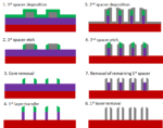
Self-aligned quadruple patterning (SAQP) is the most widely available technology used for patterning feature pitches less than 38 nm, with a projected capability to reach 19 nm pitch. It is actually an integration of multiple process steps, already being used to pattern the fins of FinFETs [1] and 1X DRAM [2]. These steps, shown… Read More
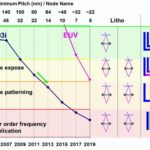
In a previous article [1], the Rayleigh criterion was mentioned as the resolution limit for the distance between two features. On the other hand, in a following article [2], the minimum pitch was mentioned for the resolution limit for arrayed features. In this article, we reconcile the two by considering gaps between arrayed features,… Read More
State-of-the-art chips will always include some portions which are memory arrays, which also happen to be the densest portions of the chip. Arrayed features are the main targets for lithography evaluation, as the feature pitch is well-defined, and is directly linked to the cost scaling (more features per wafer) from generation… Read More
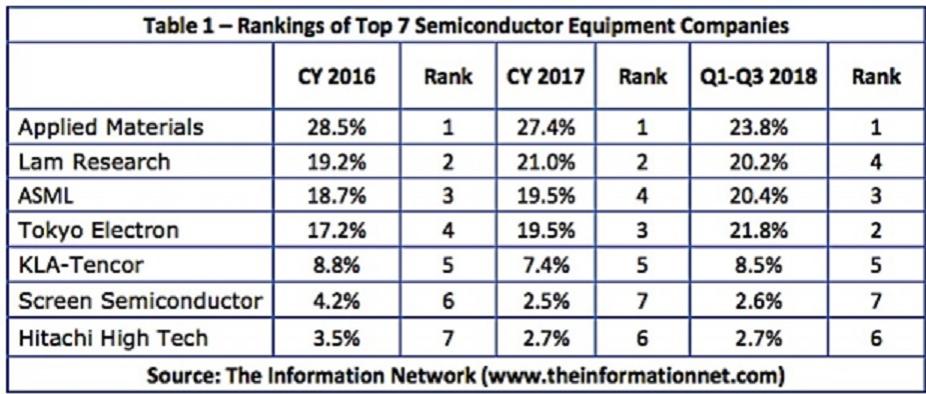
Semiconductor equipment vendor ranking, which didn’t change much between 2016 and 2017, is undergoing a makeover, as Lam Research, ASML, and Tokyo Electron (TEL) are switching places and top-ranked Applied Materials is getting closer to losing its number one ranking.
Since the 1990s, Applied Materials has been the market leader… Read More
Some of Intel’s technology posts make some pretty specific statements and I have seen a number of posts where people seem to have misinterpreted what Intel was actually saying.
Multi Patterning
I have seen a lot of confusion on this one with some people saying Intel didn’t use multi patterning at 22nm and others saying Intel used … Read More
On the Cadence booth at DAC, Lars Liebmann of IBM presented on the challenges of 10nm. As he put it, how the lithography folks are keeping things very interesting for the EDA tool development engineers. Although 14nm/16nm hasn’t yet ramped into HVM, the advanced work for tools and IP has all moved to 10nm. Although Lars gave… Read More
As you can’t have failed to notice by now, 28nm is the last process node that does not require double patterning. At 20nm and below, at least some layers require double patterning. The tightest spacing is typically not the transistors but the local interconnect and, sometimes, metal 1.
In the litho world they call double patterning… Read More
At major EDA events, CEDA (the IEEE council on EDA, I guess you already know what that bit stands for) hosts a lunch and presentation for attendees and others. This week was ICCAD and the speaker was Lars Liebmann of IBM on The Escalating Design Impact of Resolution-Challenged Lithography. Lars decided to give us a whirlwind tour … Read More