In recent advanced nodes, via and cut patterning have constituted a larger and larger portion of the overall BEOL mask count. The advent of SALELE [1,2] caused mask count to increase for EUV as well, resulting in costs no longer being competitive with DUV down to 3nm [3]. Further development by TEL [4] has shown the possibility for further mask reduction, which will be considered in this article.
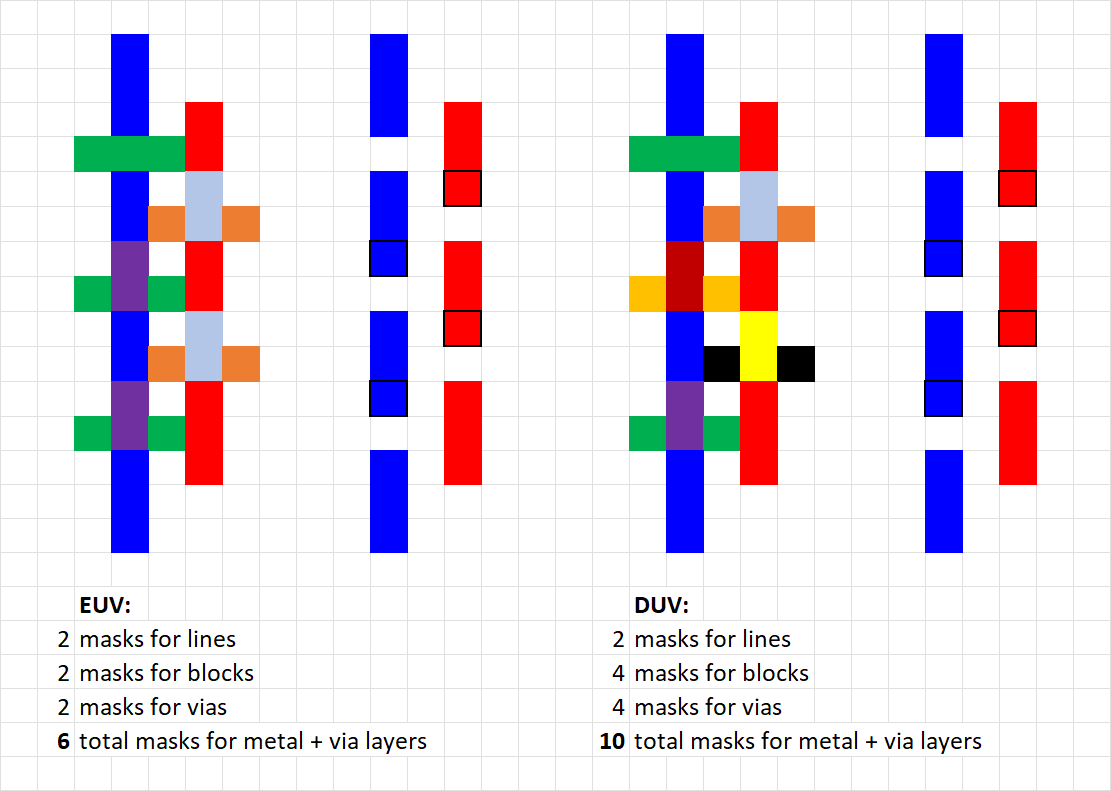
With the BEOL metal pitch approaching 20 nm, several patterning scenarios can be envisaged. The first case would be EUV SALELE (Figure 1, left). This would entail the use of 2 masks for trenches, 2 masks for blocks (cuts), and 2 masks for vias. The factor of two comes from the two etch “colors” (mutual selectivity) needed to help relax overlay requirements. If this were done by DUV (Figure 1, right), the number of block and via masks would have to double to achieve the same pitch per line or track [3]. Two masks can still be used to define (through an LELE (Litho-Etch-Litho-Etch) sequence) a core pattern upon which spacer-based SADP (self-aligned double patterning) is executed [5]. This leads to 10 masks being used for DUV vs. 6 for EUV, to pattern one metal and one via layer. While there are more steps, the cost still favors DUV [3]. Still, we can check if there is any opportunity to reduce the masking steps.

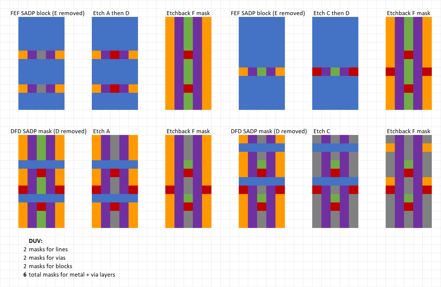
The number of DUV masks for blocking/cutting can be halved by applying SADP instead of LELE. Figure 2 is an abbreviated sketch of the expected flow.

The number of DUV masks for the trench layer (line + block/cut) is now the same as for the EUV case. While we now have extra SADP process sequences that need to be designed, the benefit is that energy consumption for DUV SADP is still ~30% less than that for an EUV single exposure [6], while not being expected to be more expensive [7].
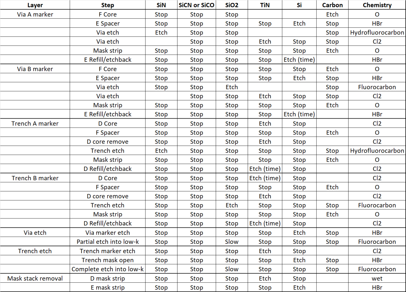
Focusing now on via mask reduction, we can apply the SADP replacement of LELE there as well. With SADP being applied to the trench, via, and block layers successively, the etch selectivity of the materials being processed must be considered very carefully. The resulting process step sequence (Figure 3) becomes much more complicated of course, but the end result would be a halving of the via masks (Figure 4).


Thus, the mask reduction is carried to its extreme, by greatly increasing the etch complexity. Yet, even without going so far, having extra DUV masks should not be prohibitive in any way.
References
[1] R. Venkatesan et al., Proc. SPIE 12292, 1229202 (2022).
[2] Y. Drissi et al., Proc. SPIE 10962, 109620V (2019).
[3] F. Chen, https://www.linkedin.com/pulse/extension-duv-multipatterning-toward-3nm-frederick-chen
[4] A. J. deVilliers, US9240329; H. Kang, A. J. deVilliers, US10115726.
[5] S. Sakhare et al., Proc. SPIE 9427, 94270O (2015).
[6] L-A. Ragnarsson et al., “The Environmental Impact of CMOS Logic Technologies,” 2022 EDTM.
[7] L. Liebmann et al., Proc. SPIE 9427, 942702 (2015).
[8] Y. Zhang et al., JVST A14, 2127 (1996).
[9] A. Sankaran and M. Kushner, JAP 97, 023307 (2005).
[10] S. A. Vitale et al., JVST B 27, 2472 (2009).
[11] B. S. Kwon et al., J. Electrochem. Soc. 157, D135 (2010).
[12] J. S. Kim et al., JVST A28, 65 (2010).
[13] F. Weilnboeck et al., JVST B 30, 041811 (2012).
[14] S. Dhungana et al., JVST A34, 061302 (2016).
[15] D. Radisic et al., Proc. SPIE 10963, 109630P (2019).
[16] K-C. Chien and C-H. Chang, JVST B 40, 062802 (2022).
[17] N. Miyoshi et al., JVST A 40, 032601 (2022).
This article first appeared in LinkedIn Pulse: BEOL Mask Reduction Using Spacer-Defined Vias and Cuts
Also Read:
Predicting Stochastic Defectivity from Intel’s EUV Resist Electron Scattering Model
The Significance of Point Spread Functions with Stochastic Behavior in Electron-Beam Lithography
Extension of DUV Multipatterning Toward 3nm
Share this post via:


Solving the EDA tool fragmentation crisis