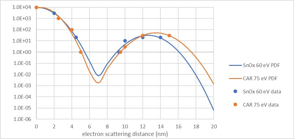
The release and scattering of photoelectrons and secondary electrons in EUV resists has often been glossed over in most studies in EUV lithography, despite being a fundamental factor in the image formation. Fortunately, Intel has provided us with a laboriously simulated electron release and scattering model, using the GEANT4 Monte Carlo simulator toolkit [1]. The simulator is able to track and keep statistics on all photons and released photoelectrons and secondary electrons and their trajectories. Consequently, it is possible to obtain the probability density for a given scattering distance at a given electron energy. In the resists studied, there were certain electron energies within the covered 10-82eV range where it was especially easy to trace electron scattering distances. Figure 1 shows the double Gaussian fitted probability density function for a 60 eV electron in SnOx resist and a 75 eV electron in chemically amplified resist.

Figure 1. Probability density functions for electron scattering distance for a 75 eV electron in chemically amplified resist (CAR) and 60 eV electron in SnOx. 25 mJ/cm2 EUV dose to a 100 nm x 100 nm patch of resist 50 nm thick. Data points sourced from Figure 7 of Ref. [1].
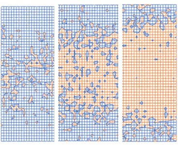
It is possible to get the population fraction beyond a given electron scattering distance, using the weighted average cumulative distribution functions of the two Gaussians. For example, a population fraction of 1e-11 goes beyond 20 nm for the 75 eV electron in CAR or the 60 eV electron in SnOx. This large electron scattering distance is a source of blur. Blur aggravates the impact of stochastic dose fluctuations because the peaks and valleys of the image are partly flattened by blur. A blur of 20 nm substantially destroys a 50 nm pitch image (Figure 2), regardless of exposure threshold, i.e., exposed critical dimension (CD). Essentially, there is a defect floor. For the smaller exposed CD, there is mostly unexposed area within the exposed region. For the larger exposed CD, there are exposed spots in the unexposed region.

Figure 2. Stochastic defectivity with decreasing resist exposure threshold (wider exposed CD), going from left to right. Exposure conditions: 50 nm pitch, 20 nm blur, 30 mJ/cm2 absorbed, secondary electron quantum yield=8. Pixel size: 1 nm x nm. More details in Refs. [2].
A defect probability of 1e-11 corresponds to a 1000 nm2 defective area per cm2 area. Or it can also mean, for example, one missing contact out of 100 billion contacts. When the blur probability matches the defect probability as in this case, we get a measure of the stochastic defectivity. A higher probability for defect-inducing blur can occur for smaller blur values, and this would happen for a smaller pitch. For the blur to play much less of a role in aggravating stochastic defectivity, the pitch has to be substantially larger than the blur. This also has the simultaneous benefit of making the stochastic fluctuations less significant by having more absorbed photons (per nm) per pitch.
References
[1] P. Theofanis et al., “Modeling photo, electron, and chemical interactions in a model hafnium oxide nanocluster EUV photoresist,” Proc. SPIE 11323, 113230I (2020).
[2] F. Chen, “Modeling EUV Stochastic Defects With Secondary Electron Blur,” https://www.linkedin.com/pulse/modeling-euv-stochastic-defects-secondary-electron-blur-chen/ (2023); also F. Chen, “EUV Stochastic Defects from Secondary Electron Blur Increasing With Dose,” https://www.youtube.com/watch?v=Q169SHHRvXE&t=94s (2023).
This article first appeared in LinkedIn Pulse: Predicting Stochastic Density from Intel’s EUV Resist Electron Scatterning Model
Also Read:
The Significance of Point Spread Functions with Stochastic Behavior in Electron-Beam Lithography
Extension of DUV Multipatterning Toward 3nm
Stochastic Model for Acid Diffusion in DUV Chemically Amplified Resists
Share this post via:


Solving the EDA tool fragmentation crisis