You are currently viewing SemiWiki as a guest which gives you limited access to the site. To view blog comments and experience other SemiWiki features you must be a registered member. Registration is fast, simple, and absolutely free so please,
join our community today!
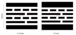
At IEDM 2019, TSMC revealed two versions of 5nm standard cell layouts: a 5.5-track DUV-patterned version and a 6-track EUV-patterned version [1]. Although the metal pitches were not explicitly stated, later analyses of a 5nm product, namely, Apple’s A15 Bionic chip, revealed a cell height of 210 nm [2]. For the 6-track … Read More
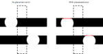
Spacer-defined patterning is an expected requirement for advanced semiconductor patterning nodes with feature sizes of 25 nm or less. As the required gaps between features go well below the lithography tool’s resolution limit, the use of cut exposures to separate features is used more often, especially in chips produced… Read More
The intricacies of analog IP circuit design have always required special consideration during physical layout. The need for optimum device and/or cell matching on critical circuit topologies necessitates unique layout styles. The complex lithographic design rules of current FinFET process nodes impose additional restrictions… Read More
On Tuesday evening December 8[SUP]th[/SUP] at IEDM, Coventor held a panel discussion entitled the “The last half nanometer”. Coventor is a leading provider of simulation software used to design processes. This is my third year attending the Coventor panel discussion at IEDM and they are always excellent with very strong panels… Read More
In the first installment of this series on Moore’s law we examined what Moore’s law is and presented some data on how it has affected the industry. In this installment we will discuss the manufacturing cost reduction strategies that have made Moore’s law possible.
Manufacturing Cost Drivers
The manufacturing cost of a semiconductor… Read More