You are currently viewing SemiWiki as a guest which gives you limited access to the site. To view blog comments and experience other SemiWiki features you must be a registered member. Registration is fast, simple, and absolutely free so please,
join our community today!
For many years, monolithic chips defined semiconductor innovation. New microprocessors defined new markets, as did new graphics processors, and cell-phone chips. Getting to the next node was the goal, and when the foundry shipped a working part victory was declared. As we know, this is changing. Semiconductor innovation is… Read More
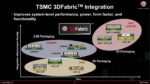
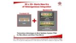
Last week TSMC announced the opening of an advanced backend fab for the expansion of the TSMC 3DFabric System Integration Technology. It’s a significant announcement as the chip packaging arms race with Intel and Samsung is heating up.
Fab 6 is TSMC’s first all-in-one advanced packaging and testing fab which is part of the… Read More
TSMC’s 3DFabric initiative was a big focus at the symposium, as it should be. I remember when TSMC first went public with CoWos the semiconductor ecosystem, including yours truly, let out a collective sigh wondering why TSMC is venturing into the comparatively low margin world of packaging. Now we know why and it is absolutely… Read More
TSMC recently held their 10th annual Open Innovation Platform (OIP) Ecosystem Forum. An earlier article summarized the highlights of the keynote presentation from L.C. Lu, TSMC Fellow and Vice-President, Design and Technology Platform, entitled “TSMC and Its Ecosystem for Innovation” (link).
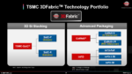
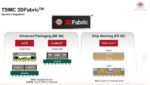
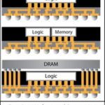
Overview of 3D Fabric
The TSMC… Read More
The recent TSMC Technology Symposium provided several announcements relative to their advanced packaging offerings.
General
3DFabricTM
Last year, TSMC merged their 2.5D and 3D package offerings into a single, encompassing brand – 3DFabric.
2.5D package technology – CoWoS
The 2.5D packaging options are divided into the CoWoS… Read More
TSMC as Pure Play Wafer Foundry
TSMC started its wafer foundry business more than 30 years ago. Visionary management and creative engineering teams developed leading-edge process technologies and their reputation as trusted source for high-volume production. TSMC also recognized very early the importance of building an … Read More
Regular Semiwiki readers are aware of the rapid emergence of various (multi-die) advanced package technologies, such as: FOWLP (e.g., Amkor’s SWIFT, TSMC’s InFO); 2D die placement on a rigid substrate (e.g., TSMC’s CoWoS); and, 2.5D “stacked die” with vertical vias (e.g., any of the High Bandwidth Memory,… Read More
I caught up with John Ferguson of Mentor Graphics this week to learn more about a recent announcement that TSMC has extended its collaboration with Mentor in the area of Fan-Out Wafer Level Processing (FOWLP).
In March of last year Mentor and TSMC announced that they were collaborating on a design and verification flow for TSMC’s… Read More
It is that time again, time for the originators of the pure-play foundry business to update their top customers and partners on the latest process technology developments and schedules. More specifically, all of the TSMC FinFET processes (16nm, 10nm, 7nm, and beyond), TSMC IP portfolio (CMOS image sensor, Embedded Flash, Power… Read More
Recent reports have Intel displacing Qualcomm as the modem supplier and TSMC as the foundry for the next Apple A10 SoC. That is if you call this a credible report: … Read More