

Daniel Nenni was gracious enough to encourage me to conduct a brief webinar describing a new reference text, recently published by Prentice-Hall, part of the Semiwiki Webinar Series.
VLSI DESIGN Methodology Development Webiner Replay
Background
I was motivated to write the text to provide college students with a broad background on SoC design. My experience with hiring new college microelectronics grads was that they typically received a good introduction to CMOS logic circuits, although likely using a somewhat dated text. Yet, the students often have not been exposed to a full SoC design and analysis methodology.
Specifically, there have been recent methodology enhancements driven by technology node evolution that students would benefit from including in their curriculum:
- hard and soft IP integration
- voltage domain and power state definitions with a power format file
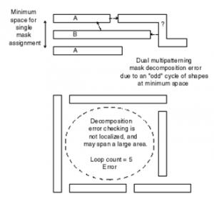
- multipatterning lithography, other lithography restrictions (unidirectional wires, forbidden pitches, via/contact size options)
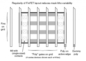
- characteristics of FinFET-based circuit design
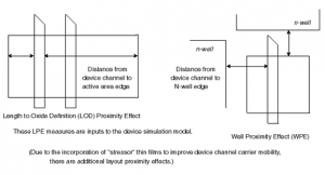
- electrical analysis with layout-dependent effects, (global and local) process variation
The goal was to provide students with an up-to-date SoC design perspective. Examples of figures from the text are appended below.
Layout Dependent Effects in device models
Multipatterning decomposition and “odd cycle DRC check”
FinFET layout example
The industry experts that reviewed the text for Prentice-Hall indicated that professional engineers would likely find material of interest. They asked that the text also include some practical subjects and examples. As a result, there are discussions on topics such as:
- managing ECO’s
- executing silicon bring-up and debug
- SoC project management
A few cases of SoC project setbacks are provided, as well.
The webinar will briefly review the organization and context of the text, highlighting some of the unique topics associated with leading process nodes. A general Q&A session will follow that introduction.
Please feel free to register for the webinar, using the link on the left side of the semiwiki.com home page.
-chipguy
PS. There is also a website where readers can provide comments, and identify (hopefully few) errata: http://www.vlsidesignmethodology.com .
Any feedback on the text would definitely be most welcome. Thanks in advance!
VLSI DESIGN Methodology Development Webiner Replay


TSMC CoWoS versus Intel EMIB Semiconductor Packaging