
The pace of Moore’s Law scaling for monolithic integrated circuit density has abated, due to a combination of fundamental technical challenges and financial considerations. Yet, from an architectural perspective, the diversity in end product requirements continues to grow. New heterogeneous processing units are being employed to optimize data-centric applications. The traditional processor-memory interface latencies are an impediment to the performance throughput needed for these application markets. Regular Semiwiki readers are aware of the recent advances in advanced multi-chip package (MCP) offerings, with 2.5D interposer-based and 3D through-silicon via based topologies.
Yet, it wasn’t clear – to me, at least – how quickly these offerings would be embraced and how aggressively customers would push the scope of multi-die integration for their design architectures. I recently had the opportunity to attend an Advanced Packaging Workshop conducted by Intel. After the workshop, I concluded that the rate at which advanced MCP designs are pursued will accelerate dramatically.
At the workshop, the most compelling indication of this technology growth was provided by Ram Viswanath, Vice President, Intel Assembly/Test Technology Development (ATTD). Ram indicated, “We have developed unique 3D and 2.5D packaging technologies that we are eager to share with customers. Product architects now have the ability to pursue MCP’s that will offer unprecedented scale and functional diversity.” The comment caught the audience by surprise – several members asked Ram to confirm. Yes, the world’s largest semiconductor IDM is enthusiastically pursuing collaborative MCP designs with customers.
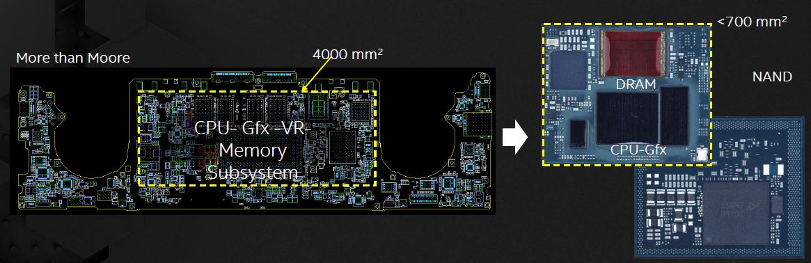
For example, the conceptual figure below depicts a CPU, GPU, VR accelerator, and memory architecture integrated into a package that is one-sixth the dimension associated with a discrete implementation. The size of this organic package is potentially very large – say, up to 100mm x 100mm. (Intel’s Cascade Lake server module from the Xeon family is a 76mm x 72.5mm MCP containing two “full reticle-size” processor die.)
For the cynical reader, this was not the same atmosphere as the previous announcement of the fledgling Intel Custom Foundry fab services. There was a clear, concise message that emerging data-driven applications will want to leverage multi-chip package integration (around an Intel CPU or FPGA). The Intel ATTD business unit is committed to support these unique customer designs.
The rest of this article will go into a bit of the MCP history at Intel, with details on the 2.5D and 3D package technologies, as well as some future packaging research underway.
MCP History
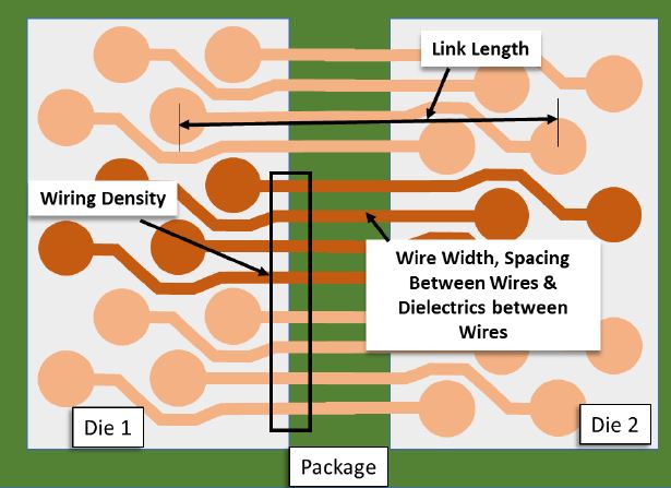
After the workshop, I followed up with Ram V., who provided a wealth of insights into the R&D activity that has been invested in MCP technology development at Intel. He indicated, “There is extensive experience with multi-chip packaging at Intel. For example, we are shipping a unique embedded silicon bridge technology for inter-die package connectivity, which has been in development for over a decade. This capability to provide wide interface connectivity between die offers low pJ/bit power dissipation, low signal integrity loss between die, and at low cost.” The figure below depicts the interconnect traces between the microbumps of adjacent die edges – a key metric is the (product of the) areal bump density and routable embedded traces per mm of die perimeter.
“The technology development focused on embedding a silicon bridge into the panel-based organic package assembly flow. The x, y, z, and theta registration requirements for the bridge are extremely demanding.”, Ram continued.
Ram showed examples of Stratix FPGA modules with HBM memory utilizing the embedded bridge. “This product roadmap began with just a few SKU’s when Intel was fabricating Altera FPGA’s, prior to the acquisition. FPGA applications have grown significantly since then – there are now MCP offerings throughout the Stratix product line.” He also showed (unencapsulated) examples of the recently-announced Kaby Lake CPU modules with external GPU, leveraging embedded bridges between die.
“Any significant assembly or reliability issues with the die from various fabs?”, I asked.
“This technology is the result of a collaborative development with suppliers.”, he replied. Pointing to different die in the various MCP modules, he continued, “This one is from TSMC. This one is from GF. Here are HBM memory stacks from SK Hynix. We have worked closely with all the suppliers on the specifications for the micro-bump metallurgy, the volume of bump material, the BEOL dielectric material properties, die thickness and warpage. All these sources have been qualified.”
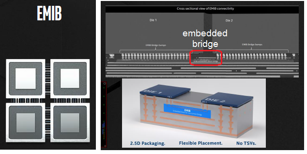
EMIB
The embedded multi-die interconnect bridge (EMIB) is a small piece of silicon developed to provide wide interconnectivity between adjacent edges of two die in the MCP. The EMIB currently integrates four metallization planes – 2 signal and 2 power/ground (primarily for shielding, but could also be used for P/G distribution between die).
Additionally, the SI team at Intel has analyzed the signal losses for different interconnect topologies of signal and ground traces of various lengths – see the figure below.

Ravi Mahajan, Intel Fellow, provided additional technical information on EMIB. He indicated the metal thickness of the EMIB planes is between that of silicon die RDL layers and package traces, achieving a balance between interconnect pitch and loss characteristics. “We’re at 2um/2um L/S, working toward 1um/1um. Our SI analysis for the EMIB suggests up to an 8mm length will provide sufficient eye diagram margin. Conceptually, an EMIB could up to ~200mm**2.” (e.g., 25mm between adjacent die edges X 8 mm wide)
Currently, the design and fabrication of the bridge is done by Intel ATTD – there is no external design kit, per se. “The development of the I/O pad floorplans for the adjacent die with the embedded bridge at ATTD is a collaborative effort.”, Ram indicated. “There is also significant cooperation on the design of the VDDIO and GNDIO power delivery through the package and around the EMIB to the perimeter bump arrays on the die. Intel ATTD also does the thermal and mechanical integrity analysis of the composite package design. As the thermal dissipation levels of the emerging markets for MPC’s can be high, and due to the different thermal coefficient of expansion between the die and EMIB silicon and the organic substrate, thermal and mechanical analysis of the microbump attach interface is critical.”
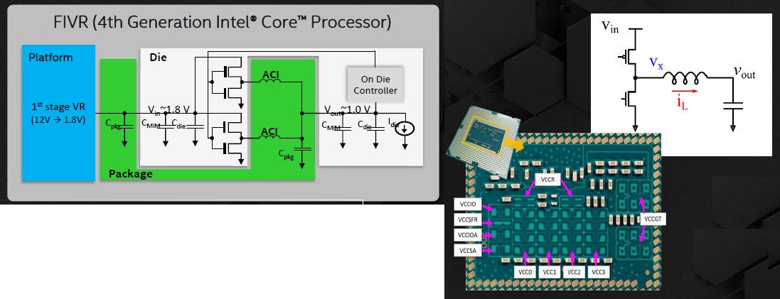
It is probably evident, but worth mentioning that the presence of the EMIB silicon in the package does not interfere with the traditional process for adding surface-mount passives to the overall assembly (e.g., decoupling caps). At the workshop, the support for backside package metal loop inductors and SMT caps was highlighted – “Intel CPU packages have integrated voltage regulation and voltage domain control since the 22nm process node. The inductor and capacitor elements on the package are part of the buck converter used in the regulator design.”, Ram indicated. Customers for Intel MCP designs would have this capability, as well.
Note the characteristics of the EMIB-based design differ considerably from the 2.5D package offerings utilizing a silicon interposer. On the one hand, the Si interposer allows greater flexibility in inter-die connectivity, as the interposer spans the extent of the entire assembly. (Newer 2.5D offerings are ‘stitching’ the connection traces between reticle exposures to provide an interposer design greater than the 1X maximum reticle field dimensions.) Conversely, the EMIB approach is focused on adjacent die edge (wide, parallel) connectivity. The integration of multiple bridges into the conventional package assembly and final encapsulation flow enables a large area field – e.g., a 100mm X 100mm dimension on a 500mm X 500mm organic substrate panel that was mentioned during the workshop. The EMIB with organic substrate provides a definite cost optimization.
3D “Foveros”
With the Lakefield CPU product family, Intel introduced 3D die-stacked package offerings, utilizing through silicon vias. The figure below illustrates the 3D die stacks.
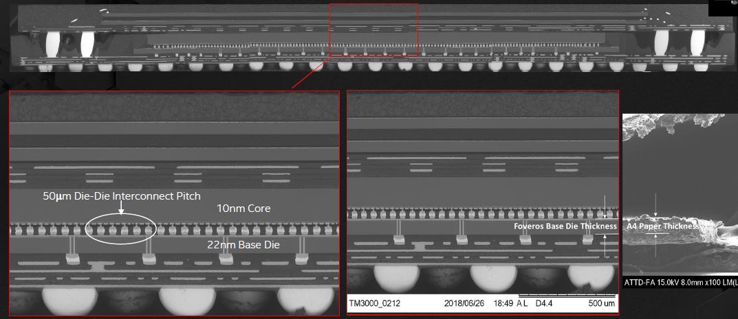
Advanced packaging R&D investment is focused on reducing both the TSV and microbump pitch dimensions – currently at a 50um pitch, heading to ~30-35um pitch. This will necessitate a transition from thermo compression bonding to a unique “hybrid bonding” process – see the figure below.
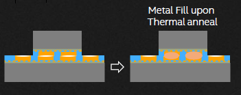
Whereas thermo compression bonding utilizes pressure and temperature to meld exposed pad metallurgies on the two die faces, hybrid bonding starts with a (somewhat esoteric) polishing process to provide pad metals with precisely controlled “dishing” of a few nanometers at the die surface. The bonding step utilizes van der Waals forces between the (hydrophilic, extremely planar) die surfaces, then expands the metals during annealing to result in the pad connection.
Another key 3D packaging R&D concern centers around scaling the (base) die thickness – the goal for advanced 3D packages is to aggressively scale the Z-height of the final assembly. “Thinning of the stacked die exacerbates assembly and reliability issues.”, Ravi M. highlighted. As an interesting visual example, he said, “Consider the handling and warpage requirements for die no thicker than a sheet of A4 paper.” (Starting 300mm wafer thickness: ~775um; A4 paper sheet thickness: ~50um)
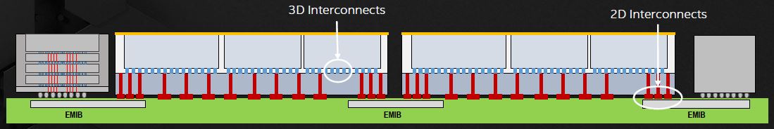
In the near future, the ability to combine multiple 3D die stacks as part of a large 2.5D topology will be available, a configuration Intel ATTD denoted as “co-EMIB”. The figure below illustrates the concept of a combination of 3D stacked die with the embedded bridge between stacks.
Chiplets, KGD’s, and AIB
The accelerated adoption of MCP technology will rely upon the availability of a broad offering of chiplets, in a manner similar to the hard IP functionality in an SoC. As mentioned above, the Intel ATTD team has already addressed the physical materials issues with the major silicon sources, to ensure high assembly/test yields and reliability. Yet, the electrical and functional interface definition between chiplet I/O needs an industry-wide focused effort on standardization, to ensure chiplet interoperability.
Intel has released the AIB specification into the public domain, and is an active participant in the DARPA “CHIPS” program to promote chiplet standards. (DARPA link, AIB link — registration required) Somewhat surprisingly, the IEEE does not appear to be as actively engaged in this standard activity – soon, no doubt.
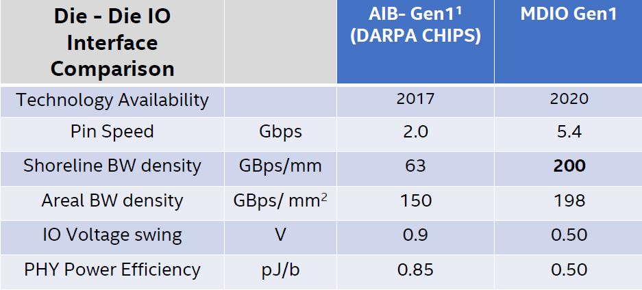
At the workshop, the Intel ATTD team indicated that internal activities are well underway on the next gen chiplet interface spec (MDIO), targeting an increase in data rate from 2Gbps to 5.4Gbps (at a lower voltage swing to optimize power).
MCP product designs will continue, but the growth in adoption necessitates a definitive standard – an “Ethernet for chiplet interconnectivity”, as described by Andreas Olofsson from DARPA.
There is another facet to chiplet-based designs that was discussed briefly at the workshop. The final, post burn-in test yield of the MCP will depend upon the test and reliability characteristics of the known good die (KGD) chiplets. The ATTD team indicated that Intel has made a long-standing (internal) investment in production ATE equipment development. One of the specific features highlighted was the capability to perform accelerated temperature cycling testing at wafer level, to quickly identify/sort infant fails – this the resulting KGD forwarded to package assembly will not present a major yield loss after final burn-in. The suppliers of chiplet “IP” will also certainly need to address how to provide high reliability die, at low test cost.
Futures
The final workshop presentation was from Johanna Swan, Intel Fellow, who described some of the advanced packaging R&D activities underway. The most compelling opportunity would be to alter the trace-to-via connectivity process. Rather than the large via pad-to-trace size disparity depicted in the figure above, a “zero misaligned via” would enable significant improvement in interconnect density. The figure below illustrates the current package trace-via topology, and the new ZMV trace-via connection at 2-4um trace widths.
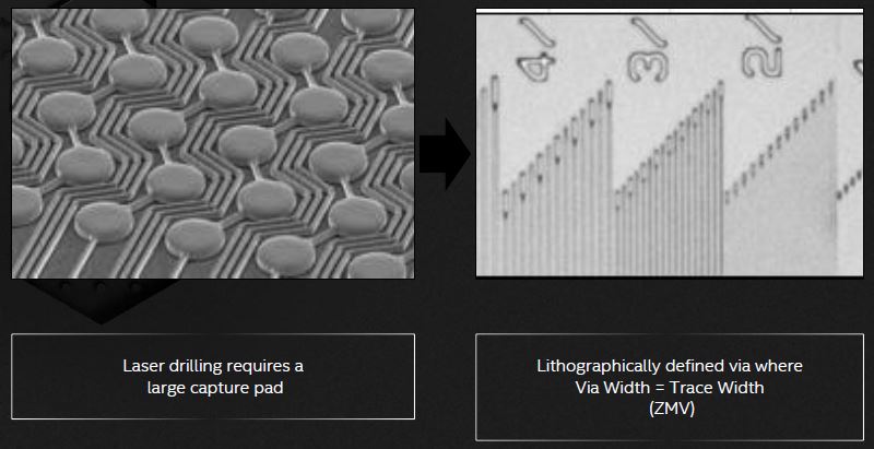
The current epoxy-based package panel utilizes laser-drilled vias – to realize a ZMV, a new technology is under research. (Johanna indicated that photoimagable materials of the polyimide family would provide the via density, but that materials, process, and cost constraints require staying with epoxy-based panels – a unique via-in-epoxy process is needed.) If the ZMV technology transitions to production, the MCP interconnect (line + space) trace density would be substantially increased – when combined with improvements in microbump pitch, the system-level functionality realizable in a large MCP would be extremely impressive.
Summary
There were three key takeaways from the workshop.
- Heterogeneous multi-chip (die and/or chiplet) packaging will introduce tremendous opportunities for system architects to pursue power/perf/area + volume/cost optimizations.
- The Intel EMIB interconnect bridge at die interfaces offers a unique set of cost/size/complexity tradeoffs compared to a 2.5D package incorporating a silicon interposer.
- The Intel ATTD team is committed to supporting their advanced 2.5D, 3D, and merged (co-EMIB) technologies for customers seeking unique product solutions to data-driven markets.
Frankly, in the recent history of microelectronics, I cannot think of a more interesting time to be a product architect.
-chipguy
Share this post via:


Comments
6 Replies to “The Coming Tsunami in Multi-chip Packaging”
You must register or log in to view/post comments.