You are currently viewing SemiWiki as a guest which gives you limited access to the site. To view blog comments and experience other SemiWiki features you must be a registered member. Registration is fast, simple, and absolutely free so please,
join our community today!
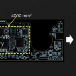
Traditional methods of chip design and packaging are running out of steam to fulfill growing demands for lower power, faster data rates, and higher integration density. Designers across many industries – like 5G, AI/ML, autonomous vehicles, and high-performance computing – are striving to adopt 3D semiconductor… Read More
If, like me, you’ve been paying too little attention to historically less glamorous areas of chip design like packaging, you’ll wake up one day and realize just how much things have changed and continue to advance and how interesting it’s become.
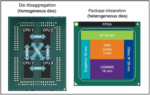
One of the main drivers here is the increasing use of chiplets to counter the decreasing… Read More
Synopsys has released a Technical Bulletin entitled “Parallel-Based PHY IP for Die-to-Die Connectivity”. The piece is authored by Manuel Mota, senior product marketing manager, staff at Synopsys. Manuel has worked at Synopsys for 11 years in the IP area. Prior to that, he worked at MIPS Technologies, Chipidea (acquired… Read More
Summary
The growing significance of ultra-short reach (USR) interfaces on 2.5D packaging technology has led to a variety of electrical definitions and circuit implementations. TSMC recently presented the approach adopted by their IP development team, for a parallel-bus, clock-forwarded USR interface to optimize power/performance/area… Read More
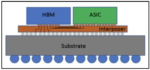
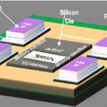
I have been watching the trend for quite some time now that many advanced FinFET designs today are actually 2.5D systems in package. All of these 2.5D silicon interposer-based designs have high-bandwidth memory (HBM) stacks on board. Often there are multiple memory stacks in both 4-high and 8-high configurations. If you follow… Read More
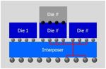
Frequent Semiwiki readers are no doubt familiar with the rapid advances in 2.5D heterogeneous multi-die packaging technology. A relatively well-established product sector utilizing this technology is the 2.5D integration of logic die with a high-bandwidth memory (HBM) DRAM die stack on a silicon interposer; the interposer… Read More
The pace of Moore’s Law scaling for monolithic integrated circuit density has abated, due to a combination of fundamental technical challenges and financial considerations. Yet, from an architectural perspective, the diversity in end product requirements continues to grow. New heterogeneous processing units are being… Read More
Years ago my good friend Herb Reiter promoted the importance of 2.5D packaging to anybody and everybody who would listen including myself. Today Herb’s vision is in production and the topic of many papers, webinars, and conferences. According to Herb, and I agree completely, advanced IC packaging is an important technology for… Read More
There’s been a lot of discussion of late about deep learning technology and its impact on many markets and products. A lot of the technology under discussion is basically hardware implementations of neural networks, a concept that’s been around for a while.
What’s new is the compute power that advanced semiconductor technology… Read More
When someone says, “2.5D packaging” my first thought is TSMC and my second thought is Herb Reiter. Herb has more than 40 years of semiconductor experience and he has been a tireless promoter of 2.5D packaging for many years. Herb writes for and works with industry organizations on 2.5D work groups and events at conferences… Read More