Synopsys has released a Technical Bulletin entitled “Parallel-Based PHY IP for Die-to-Die Connectivity”. The piece is authored by Manuel Mota, senior product marketing manager, staff at Synopsys. Manuel has worked at Synopsys for 11 years in the IP area. Prior to that, he worked at MIPS Technologies, Chipidea (acquired by Synopsys) and CERN. Clearly Manuel has a lot of background in high-performance data communications, so I paid attention to this Technical Bulletin.
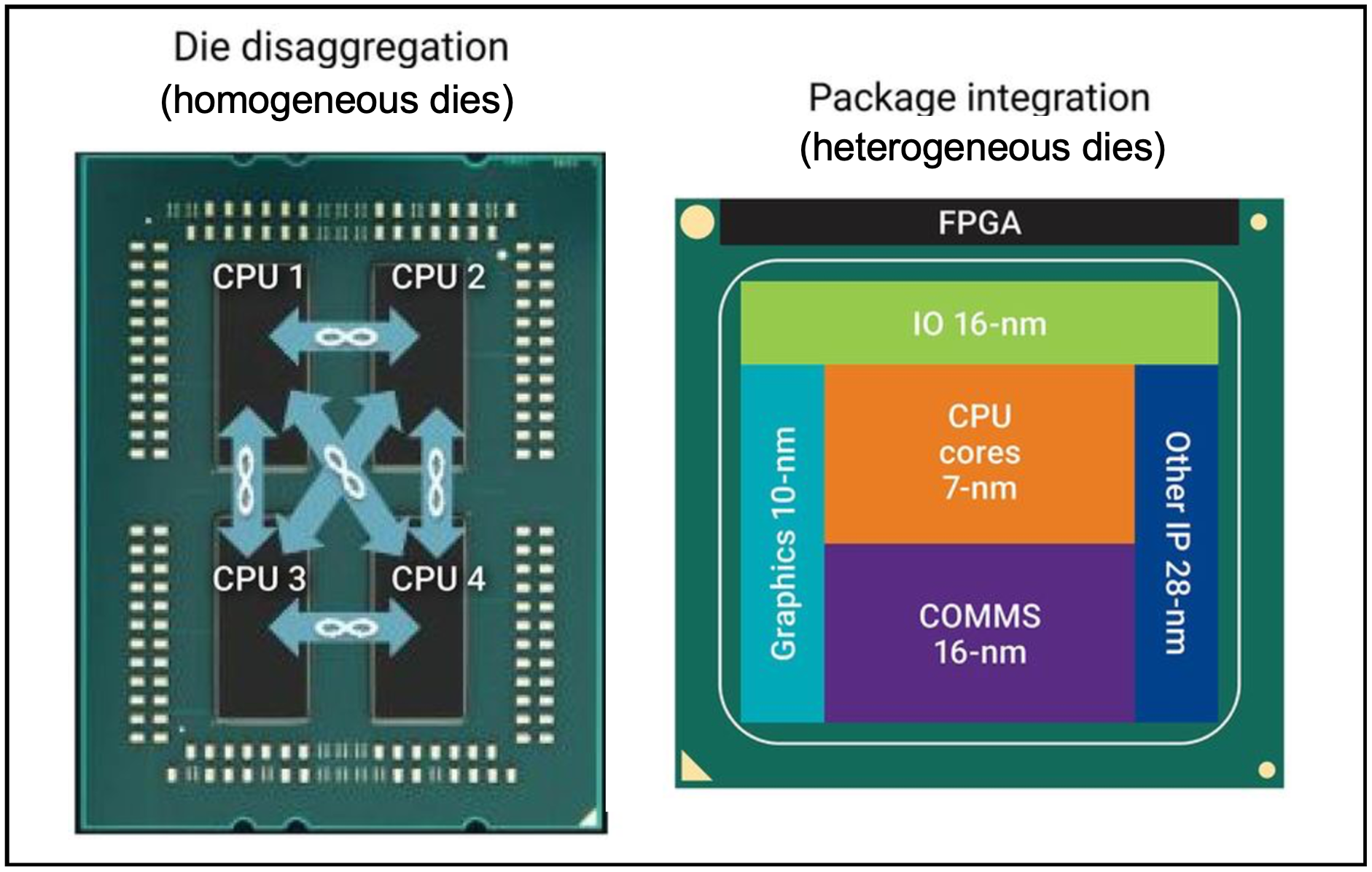
The piece begins with motivation for multi-chip package integration. There are two threads here. One is to integrate homogeneous die to facilitate splitting a larger chip into smaller pieces to manage fabrication yield. This approach also allows multiple SKUs of the design to be created easily by integrating different numbers of sub-chips. This is a very effective approach. While I was at eSilicon we did this kind of chip decomposition for a networking customer. The approach works quite well.
Another use of the multi-chip approach is to facilitate tight heterogeneous die integration to take advantage of process technologies that are cost-optimized for the implemented function. These two approaches are summarized in the graphic, above and this general integration approach is referred to as 2.5D.
Further decomposing the problem, there are two ways to implement communication between the die in a 2.5D design – high-speed serial (e.g., SerDes) or lower speed parallel interfaces. Synopsys offers IP to support both approaches and this Technical Bulletin focuses on the parallel approach. No matter which approach is used, several key characteristics must be met. These include:
- Very high-energy efficiency per bit transmitted
- Very low latency to mitigate the performance impact of splitting the functionality between the dies
- Link reliability (bit error rate)
- Bandwidth efficiency or the amount of die beachfront allocated to transmitting a given data rate
What type of design will be more appropriate for a parallel interface? The bulletin points out that the data rate that can be sustained across a link depends on the materials involved and the pitch. Silicon interposers can only maintain low data rates per lane of up to 6-8 gigabits per second per lane, making the use of high-speed SerDes die-to-die links unsuitable. It is here that a parallel die-to-die PHY architecture addresses the challenges of die-to-die links routed over silicon interposers.
Again, based on my experience at eSilicon, we were quite successful using our HBM PHY to integrate memory stacks on a silicon interposer. Continuing with the HBM example, the bulletin explains that, similar to high-bandwidth memory (HBM) interfaces, parallel die-to-die links aggregate up to 1,000s of pins, each transmitting data at a few Gbps. For example, if each pin can reach a data rate of 4Gbps unidirectionally, then the PHY needs 500 transmit pins and 500 receive pins to achieve a total aggregate bandwidth of two terabits per second (2Tbps bidirectional).
Given the large number of signal pins required for a parallel link, each driver and receiver need a simplistic architecture to be very energy- and area-efficient. The bulletin goes into how this is done. It also goes into area (beachfront) efficiency, robustness and testability. You will learn a lot about the comprehensive IP support Synopsys provides for parallel communication approaches. You can access Parallel-Based PHY IP for Die-to-Die Connectivity here. You can also get the complete picture of all Synopsys DesignWare Die-to-Die PHY IP Solutions here.
Also Read:
Making Full Memory IP Robust During Design
Synopsys Webinar: A Comprehensive Overview of High-Speed Data Center Communications
Share this post via:


Comments
There are no comments yet.
You must register or log in to view/post comments.