If, like me, you’ve been paying too little attention to historically less glamorous areas of chip design like packaging, you’ll wake up one day and realize just how much things have changed and continue to advance and how interesting it’s become.
One of the main drivers here is the increasing use of chiplets to counter the decreasing – indeed vanishing – cost gains from the latest process shrinks by allowing finer grain mapping of large sub-system blocks to their optimal process technology and optimise block reuse and design resources.
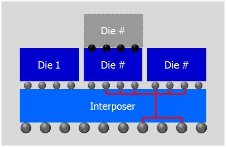
This is the sort of package scenario we’re dealing with (let’s call this an assembly of components).

The expanding world of 2.5D and 3D packaging falls between monolithic chip and PCB design, so both EDA and system level tools must be brought together to automate the process. Tasks like properly automating intra-package connectivity, checking vertical plane connections and more precise thermal modeling.
As with almost everything else in EDA these days, that means ever closer cooperation between EDA tool vendors, manufacturing and designers.
Siemens and TSMC’s work on 3DIC to jointly develop the TSMC 3Dblox standard unified design ecosystem based around Siemens’ Calibre 3DSTACK and c tools is a good example. John Ferguson’s presentation at TSMC OIP last October covered the advances here in both logical and physical verification and thermal analysis. Let’s take a closer look.
Closing the gaps in 3D Physical Verification
There are some obvious challenges here with 3DIC structures.
- Processes may share layer names, whilst having different characteristics
- Pin and pad names on components may be equivalent, but use different names
- Tools need to create a combined PV deck, netlist and physical DB to verify the entire assembly and still maintain the correct rules for individual components
- Potentially different input file formats for the components.
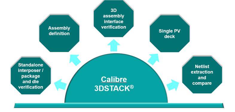
Packaging with heterogeneous process die creates new challenges for physical verification (PV), mainly in preparing a complete and accurate DB. Calibre 3DSTACK (see diagram below) already handled much of this PV prep – tasks like compiling the assembly physical DB with a single PV deck and computing the correct coupling between stacked die.

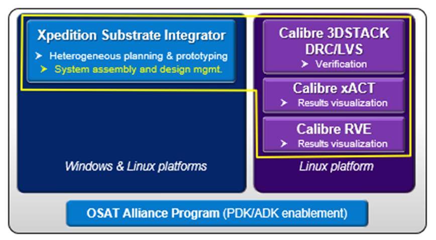
Adding Siemens’ Xpedition Substrate Integrator (XSI) planning tool closes the remaining gaps of describing the required components and connectivity (analagous to a spec or custom schematic), creating a merged netlist and managing the design DB; even automating the Calibre 3DSTACK verification.

One thing remains – finding a way to create adequate “library models” and “design rules” for the components. TSMC’s new 3DBlox approach does this with Assembly Design Kits (APDK) to describe the connectivity, process and assembly characteristics and design rules for each component.

Putting this all together we get a flow where can we prepare, run and debug the full assembly PV.

Thermal Analysis
3D packaging also creates greater thermal challenges including:
- greater interaction between die
- tougher heat dissipation challenge – greater power density due to 3D stacking
- modeling vertical thermal gradients becomes necessary
- modeling heatsink interaction for 3D die
Transistor performance strongly depends on temperature, so such thermal effects cannot be ignored. And these aren’t just signoff checks – we need good thermal and power modeling very early in the design and integrated into the ASIC design flow, since late changes here will create major rework.
With physical verification, the challenge was more one of verifying the top-level and component interfaces. Here it’s more about understanding the impact of the overall system on the components – and then how that feeds back into the top-level system.
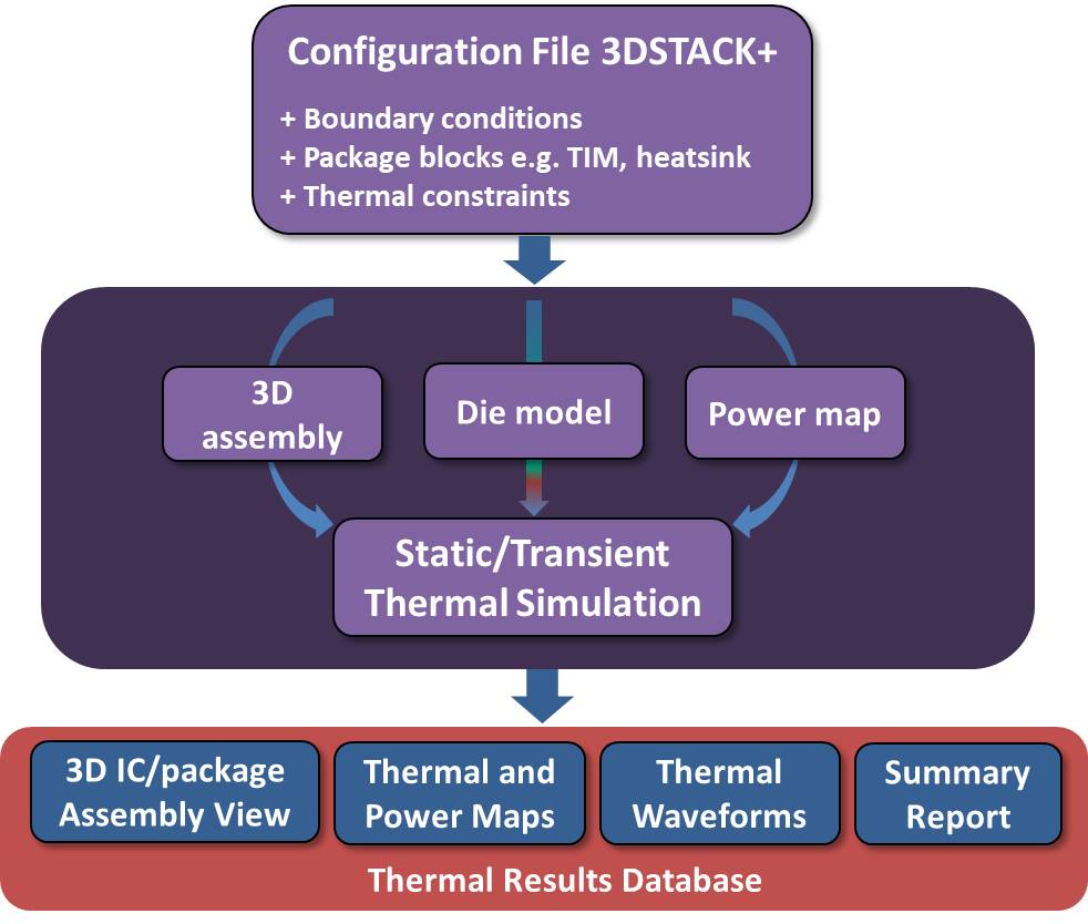
A further collaboration with TSMC extended a flow built around the existing Siemens Calibre 3DSTACK and SimCenter Flotherm tools, reusing much of the infrastructure from the PV flow.

Analysis, including static and dynamic heat maps, can be carried out at assembly, die or IP level and power analysis run using mPower. Device temperature coefficients can be extracted for more precise signal and timing analysis.
Summary
Siemens and TSMC have put together a design methodology and flow to support current and future 3DICs based on proven tools (Calibre 3DSTACK and SimCenter Flotherm and with particular attention on simplifying configuration and modeling (3DBlox) and early design use. It’s something that should continue to scale as increasingly sophisticated 3D packaging technology arrives.
It’s also noteworthy that Siemens won a TSMC OIP Partner of the Year award for this work.
Further Information
The TSMC OIP presentation (“TSMC 3Dblox™ simplifies Calibre verification and analysis”) is available until May for readers with the original event registration link and code provided by TSMC.
Find out more about Calibre physical verification and 3DSTACK here:
https://eda.sw.siemens.com/en-US/ic/calibre-design/physical-verification/
https://eda.sw.siemens.com/en-US/ic/calibre-design/physical-verification/3DSTACK/
A white paper “Taking 2.5D/3DIC physical verification to the next level” is also available.
For Siemens Flotherm thermal analysis check here:
https://www.plm.automation.siemens.com/global/en/products/simcenter/flotherm.html
Also Read:
Achieving Faster Design Verification Closure
Siemens Aspires to AI in PCB Design
Share this post via:


Comments
There are no comments yet.
You must register or log in to view/post comments.