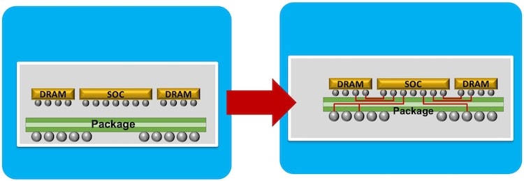
At SemiWiki we’ve written four times now about how TSMC is standardizing on a 3DIC physical flow with their approach called 3Dblox, so I watched a presentation from John Ferguson of Siemens EDA to see how their tool flow supports this with the Calibre tools. With a chiplet-based packaging flow there are new physical verification challenges, so the response at Siemens EDA was to develop Calibre 3DSTACK, which supports 3DIC and enables thermal analysis.

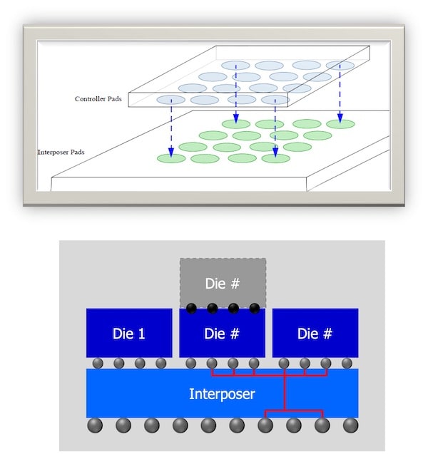
Physical checks for DRC ensure that substrate interfaces are correct with: alignment, overlaps, scaling and die-to-die spacings. LVS checking determines if connectivity through the interposer or package RDL are correct, compared to the golden netlist. Even the parasitics formed through the packaging interconnect need to be extracted and analyzed, as it impacts signal integrity and timing margins.

An early approach at 3DIC for LVS verification was to run it separately for each die to die interface, but that is impractical, instead the approach used with Calibre 3DSTACK is to check the full assembly, both DRC and LVS, with one deck, using one run.
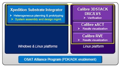
To actually design and plan your 3DIC package assembly there’s another Siemens EDA tool called Xpedition Substrate Integrator (XSI), and that allows you to create the heterogeneous rule file, plus generate the source netlist. 3DIC package design and verification tools are shown below:

TSMC supplies the Assembly Design Kits (ADK) to support their 3Dblox tool flow, where it’s like a LEF/DEF flow, but in 3 dimensions now.

Physical verification checking using the 3Dblox format is automated in this tool flow with Calibre 3DSTACK, and is independent of which tool creates the 3Dblox data.

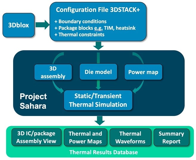
In addition to 3DIC physical verification, there are new reliability issues like thermal, as the chiplets are placed in closer proximity. Temperature increases slow down silicon switching times and shorten semiconductor lifespan, which could lead to a timing or reliability failure. To find out how the package assembly impacts each chiplet, there’s another Siemens EDA tool, Simcenter Flotherm, to support the development of a thermal digital twin. With this you can get fast analysis, while in the early planning steps. Analysis results as static or dynamic heat maps are shown at the assembly, die or IP level. You can even get a post-layout netlist with the temperature coefficients of each device, which is used for signal integrity and timing analysis.

Starting from a 3Dblox file, this thermal flow uses a 3DSTACK syntax, creating individual chip power maps across the assembly. Engineers will see wave forms or animated heat maps of the temperatures, or power can be shown at the chip or assembly level. Constraints can be specified, and then during thermal simulation any warnings or failures are noted.

Adding thermal capabilities to support 3DIC packaging at Siemens EDA required close collaboration with TSMC.
Summary
The market excitement of 3DIC design also brings about new technology challenges, like how to perform physical verification with DRC and LVS in the most efficient method. TSMC has standardized in one format, the physical stacking and logic connectivity information, calling it 3Dblox. Siemens EDA with Calibre 3DSTACK fully supports the 3Dblox format in their DRC and LVS flows. Designing and planning 3D package assemblies is done with XSI, and new thermal analysis also uses the 3Dblox format. Thermal analysis for 3DIC packaging is also possible, allowing products to be designed to meet reliability goals.
The EDA, foundry and IP communities have collaborated together to face the new 3DIC design and verification challenges, allowing our economy to enjoy a steady stream of new products that are now reaching 100 billion transistors. The future of 3DIC is bright indeed.
Related Blogs
- TSMC OIP – Enabling System Innovation
- TSMC Expands the OIP Ecosystem!
- TSMC 2022 Open Innovation Platform Ecosystem Forum Preview
- TSMC 2022 Technology Symposium Review – Advanced Packaging Development


Comments
There are no comments yet.
You must register or log in to view/post comments.