You are currently viewing SemiWiki as a guest which gives you limited access to the site. To view blog comments and experience other SemiWiki features you must be a registered member. Registration is fast, simple, and absolutely free so please,
join our community today!
At the recent TSMC Technology Symposium 2026, Siemens EDA reinforced its position as one of the key ecosystem partners supporting TSMC in the race toward AI-driven semiconductor design, advanced packaging, and next-generation process technologies. The annual forum has become one of the semiconductor industry’s most important… Read More
We all know semiconductor design is getting harder. Much harder when you consider the demands of AI workloads and heterogeneous integration of many chiplets in a single package. This class of system demands co-optimization across the entire design flow. For example, functional verification, thermal analysis, signal and power… Read More
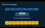
At the recent User2user conference, Amit Kumar, Principal Hardware Engineer, Microsoft, shared the company’s experience from building a 3DIC SoC and highlighted Siemens EDA tools that were used. The following is a synthesis of core aspects of that talk.
3DIC Challenges
Despite the numerous advantages of 3DIC technology, its… Read More
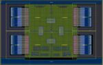
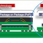
If you have anything to do with the semiconductor industry, you already know that one of the hottest areas for both manufacturing and EDA are systems designed with advanced packaging, basically putting more than one die (aka chiplets) in the same package.
When 3D packaging was first introduced, there were not really any effective… Read More
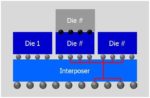
At SemiWiki we’ve written four times now about how TSMC is standardizing on a 3DIC physical flow with their approach called 3Dblox, so I watched a presentation from John Ferguson of Siemens EDA to see how their tool flow supports this with the Calibre tools. With a chiplet-based packaging flow there are new physical verification… Read More
If, like me, you’ve been paying too little attention to historically less glamorous areas of chip design like packaging, you’ll wake up one day and realize just how much things have changed and continue to advance and how interesting it’s become.
One of the main drivers here is the increasing use of chiplets to counter the decreasing… Read More
3D-IC design has become a popular discussion topic in the past few years because of the integration benefits and potential cost savings, so I wanted to learn more about how the DRC and LVS flows were being adapted. My first stop was the Global Semiconductor Alliance web site where I found a presentation about how DRC and LVS flows were… Read More