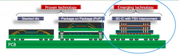

3D-IC design has become a popular discussion topic in the past few years because of the integration benefits and potential cost savings, so I wanted to learn more about how the DRC and LVS flows were being adapted. My first stop was the Global Semiconductor Alliance web site where I found a presentation about how DRC and LVS flows were extended by Mentor Graphics for the Calibre tool to handle TSV (Thru Silicon Via) technology. This extension is called Calibre 3DSTACK.

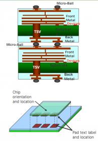
With TSV each die now becomes double-sided in terms of metal interconnect. DRC and LVS have to now verify the TSV, plus front and back metal layers.
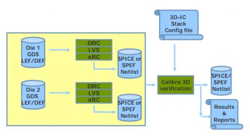
The new 3DSTACK configuration file controls DRC and LVS across the stacked die:
A second source that I read was at SOC IP where there were more details provided about the configuration file.
This rule file for the 3D stack has a list of dies with their order number, postion of each die, rotation, orientation, location of the GDS layout files and associated rule files and directories.
To do the parasitic extraction requires new information about the size and electrical properties of the microbumps, copper pillars and bonding materials.
One methodology is to first run DRC, LVS and extraction on each die separately, then add the interfaces. The interface between the stacked dies uses a separate GDS, and LVS/DRC checks are run against this GDS.
For connectivity checking between dies text labels are inserted at the interface microbump locations.
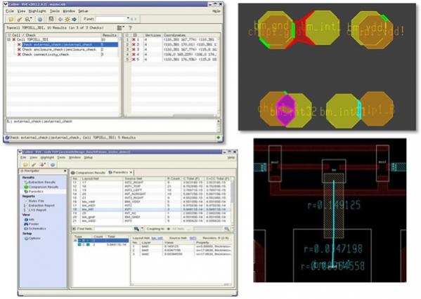
With these new 3D extensions then Calibre can run DRC, LVS and extraction on the entire 3D stack. A GUI helps you to visual the 3D rules and results from DRC, LVS and extraction:
TSMC Partner of the Year Award
Based on this extension of Calibre into the 3D realm, TSMC has just announced that Mentor was chosen as the TSMC Partner of the Year. IC designers continue to use the familiar Calibre rule decks with the added 3DSTACK technology.

Summary
Yes, 3D-IC design is a reality today where foundries and EDA companies are working together to provide tools and technology to extend 2D and 2.5D flows for DRC, LVS and extraction.
Further Info
- The GSA does have a 3D/TSV Technology Working Group.
- Video discussion from the Tech Design Forum
var _gaq = _gaq || [];
_gaq.push([‘_setAccount’, ‘UA-26895602-2’]);
_gaq.push([‘_trackPageview’]);
(function() {
var ga = document.createElement(‘script’); ga.type = ‘text/javascript’; ga.async = true;
ga.src = (‘https:’ == document.location.protocol ? ‘https://ssl’ : ‘http://www’) + ‘.google-analytics.com/ga.js’;
var s = document.getElementsByTagName(‘script’)[0]; s.parentNode.insertBefore(ga, s);
})();


Comments
0 Replies to “Physical Verification of 3D-IC Designs using TSVs”
You must register or log in to view/post comments.