
Can semiconductor devices change the temperature of the earth? The heat from my Dell XPS changes the temperature of my lap! A 63” flat screen TV changes the temperature of my living room. I just purchased six of the latest iPhones for my family (under duress) and signed up for another two years with Verizon, so our carbon footprint changes once again.

As computing goes from the desktop to the laptop to the fingertop with a total available market (TAM) of 7B+ people, power has become a critical mess. A recent Time Magazine article, 2045: The Year Man Becomes Immortal suggests that we will successfully reverse-engineer the human brain by the mid-2020s. Replicating the computing power of the human brain is one thing, unfortunately, replicating its power efficiency is quite another!
Power efficiency in the semiconductor design and manufacturing ecosystem is overwhelming design reviews: cost and power, performance and power, temperature and power, etc…. Who knows this better than Chris Malachowsky, co-founder and CTO of NVIDIA? Chris and the IEEE Council on EDA bought me lunch at ICCAD last week. Chris talked about everything from superphones to supercomputers and the semiconductor power challenges ahead.
Chris was quick to point out that NVIDIA is a processor company not a graphics (GPU) company, with $3.5B in revenue, 6,900 employees, and 2,000+ patents. Chris currently runs a 50+ PhD research group inside NVIDIA. One of the projects his group is working on is a supercomputer capable of a MILLION TRILLION calculations per second for the Department of Energy ExascaleProgram, all in the name of science. The hitch is that it can only consume 20MWs!
NVIDIA has 3 very synergistic market segments for their technology:
[LIST=1]
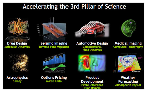
The largest market today is computer gaming at $35B+ but fingertop computing (mobile) is where the hyper growth is as it intersects all three markets. We now live in a pixel based world and whoever controls those pixels wins!
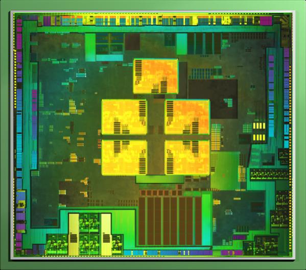
One of the worst kept secrets is NVIDIA’s new Tegra 3 architecture, which is an example of what Chris Malachowsky called a mutli-disciplinary approach to semiconductor power management. The best write-up is Anandtech’s NVIDIA’s Tegra 3 Launched: Architecture Revealed.
The Tegra 3 is a quad core SoC with almost twice the die size of its predecessor, from 49mm^2 to around 80mm^2, built on the TSMC 40nm LPG process. The performance/throughput of Tegra 3 is about five times better than last year’s Tegra 2 with 60%+ less power consumption. The Tegra 4 (code name Wayne) has already been taped out on TSMC 28nm and will appear in 2012. We will never see a better process shrink than 40nm to 28nm in regards to performance and power so expect the Tegra 4 to be extra cool and fast!
The key to the Tegra 3’s low power consumption is the fifth ARM Cortex 9 “companion” core, running at 500MHZ. You can run one to four cores at 1.3GHZ or just the companion core for background tasks, thus the power savings, and thus the mutli-disciplinary approach to low power SoC realization. You will see a flood of Tegra 3 based devices at CES in January so expect NVIDIA to have a Very Happy New Year!
The fingertop computing technology appetite is insatiable, and with a TAM of 7B+ units you can expect many more multi-disciplinary approaches to low power semiconductor design and manufacturing, believe it!


Consolidation and Competition: Who is Winning the $4.5 Billion Interface IP Race?