
If you have anything to do with the semiconductor industry, you already know that one of the hottest areas for both manufacturing and EDA are systems designed with advanced packaging, basically putting more than one die (aka chiplets) in the same package.
When 3D packaging was first introduced, there were not really any effective design tools. Obviously, each chiplet could be designed the same way as a chip would be, but it was not really possible to examine the entire design as a single system. But people managed to successfully product working designs.
Early in technology development, optimizing the pin layout for power, performance, and area take priority. High pin count ASICs/FPGAs get broken down into smaller blocks (IOs, Complex IPs, Cores, AMS blocks etc.) that are instanced many times and are integrated to form the complete floorplan of the ASIC/FPGA or chiplet. This is not only the case for ICs, but also for interposers and package substrates.
Xpedition Substrate Integrator
As designs get larger, doing all this by hand becomes less and less feasible. This is where Siemens EDA comes in with the Xpedition Substrate Integrator (xSI) IC package floor-planning and assembly tool for the design phase, and the Calibre 3DSTACK and nmDRC tools for verification.
The chiplets in a chiplet-based design have many constraints at this floorplan level. Obviously, the bumps on the chiplet need to align physically with the interposer (or interconnect bridge). Signals that leave one chiplet need to go somewhere, such as to another chiplet or out to the actual package pins, typically by way of solder balls. Clearly, this provides plenty of ways to potentially mess up.
Power Delivery Network
One specific challenge in a chiplet-based design is the power delivery network (PDN). Given that the voltage may be, say, 0.8V and the power of the system might be measured in hundreds of watts, the current involved can be hundreds of amps. Since there may be 100,000 bumps or more to carry this high current, the only practical approach is to parameterize things. Nobody is going to place 100,000 bumps by hand.
As a recent white paper from Siemens EDA, The smart path to chiplets using hierarchical device planning and pin regions, explains:
The primary power/ground domain is surprisingly simple. The region will have a specific pin pattern, pad stack definition, and a repeating signal assignment pattern (checkerboard or horizontal/vertical striped). A highly efficient way to represent this design structure is as a set of parameterized pin regions.
The white paper goes into a lot of detail on how this is accomplished, along with an example design.
Physical Design
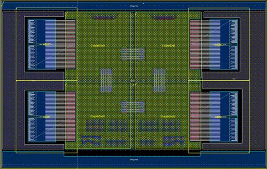
Next is to take the soft design and rearchitect into actual chiplets. The design (shown above) is The Soft IP SoC bump interface generated using parameterized pin regions containing 112,029 pins with eight power/ground domains and supporting 4-HBM interfaces.

When a design is constructed using hierarchical building blocks to represent the die-to-die interfaces along with parameterized pins to represent power distribution networks and signal patterns, the path to rearchitecting the SoC into chiplets is clear. Starting with the soft IP SoC representation, after the pins are removed, the region geometries can be quickly modified into a chiplet configuration as shown below.

With a few more steps detailed in the white paper, here is the final design complete with the HBM (high-bandwidth memory) stacks:

Summary
Package designers need to employ all the available tools to address the significant device complexity and explosion in pin count in today’s IC packaging designs, especially when early design analysis clearly detects errors. While it may still be possible to generate an initial draft of an advanced IC package design using non-graphical IC package floor-planning flows, it simply would not be feasible to keep up with the changes required by early design analysis. Siemens EDA has a portfolio of design tools that work together to deliver a correct design.
Please download the full white paper, The smart path to chiplets using hierarchical device planning and pin regions, in which a real example of a multi-die HBM-based design is used to show how package designs of complex chiplet-based designs can be created quickly and efficiently, without errors. Perhaps more importantly, iterative updates can be done in mere minutes or even seconds because of effective use of hierarchy in the design.
Also Read:
AI for the design of Custom, Analog Mixed-Signal ICs
Optimizing Shift-Left Physical Verification Flows with Calibre
Share this post via:


Comments
There are no comments yet.
You must register or log in to view/post comments.