
You are probably familiar with the acronym PPA, which stands for Power/Performance/Area. Sometimes it is PPAC, where C is for cost, since there is more to cost than just area. For example, did you know that adding an additional metal layer to a chip dramatically increases the cost, sometimes by millions of dollars? It requires a minimum of two masks (interconnect, and vias) plus all the additional associated process steps. And interconnect layers normally come in pairs, vertical and horizontal, so usually it is four masks.
There are many inputs into optimizing PPAC, and a significant one is designing the clock tree. The clock can consume a lot of the power, and a lot of the interconnect, and obviously affects performance. The process of designing the clock tree is usually called Clock Tree Synthesis, usually abbreviated to CTS. Siemens EDA recently published a white paper Placement and CTS Techniques for High-Performance Computing Designs.
One challenge EDA tools face is that you only get the true quality of results when you have finished the design. In practice, this means that tools need to either use pessimism to guard band the results, or increase accuracy by having much better correlation between the tool in use and the final results.
The white paper discusses how to solve the placement and clock tree challenges in HPC designs using the Aprisa digital implementation solution, as these steps are fundamental to achieving the desired performance metrics during place and route. While most other place-and-route tools require waiting to post-route optimization to discover the true quality of the results, Aprisa offers users excellent correlation throughout the place-and-route implementation, which allows designers to gain confidence on the results much earlier in the flow at the placement and clock tree synthesis (CTS) stages. Aprisa is ideally suited to help designers deliver HPC IC innovations faster.
Aprisa is the Siemens digital implementation solution for hierarchical and block-level designs. Under the hood, it has a detail-route-centric architecture to reduce time to design closure, partly by pulling the implications of decisions early in the design process as opposed to waiting until the design is completed to find it has problems that were introduced earlier. A key to a modern implementation flow is to have consistent timing, extraction, DRC, and more across the whole flow.
Aprisa delivers optimal performance, power and area (PPA) for advanced nodes, and it has complete support for design methodologies and optimization to achieve both lowest power and highest performance.
The white paper uses an example design, an Arm Cortex-A76 in 5nm running at 2.75 GHz, and using 12 layers of metal for interconnect. I don’t have space here to go into the design in detail, you’ll have to read the white paper for a deeper dive.
The focus of the exercise was to analyze using 10 layers of metal versus 12 layers of metal (I said interconnect layers usually come in pairs already). The analysis revealed that, for the 10-layers option, the frequency would have to be lowered by 9 percent to achieve the desired power target. However, it resulted in significant cost savings for the entire project. Obviously, Aprisa cannot make the decision for you as to whether 9% performance hit is worth it to reduce the cost.
The focus of the white paper is clock tree synthesis (CTS), one of the big challenges in any HPC design. Aprisa supports useful skew, starting at placement optimization and continuing all the way to route optimization, to make certain that challenging design frequency targets are met. A strength of Aprisa CTS technology is that the push and pull offsets generated during placement optimization are realized during clock tree implementation.
Clocks generally go to flip-flops, and an optimization that modern cell libraries include are multi-bit flip-flops with a common clock. Aprisa has the capability to merge or demerge multi-bit flip-flops and clone/declone integrated clock gates. Aprisa does this based on the timing, physical location of the cells and criticality of the paths.
Post-CTS optimization in Aprisa includes congestion recovery that recovers congestion created during clock tree synthesis. Congestion recovery is a clock-aware approach that does not degrade timing and so reduces iterations back to placement optimization that otherwise would be required.
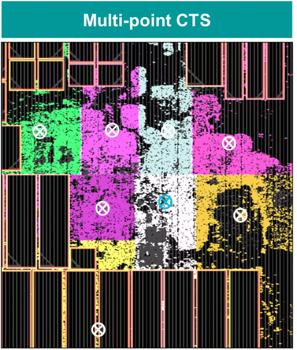
Aprisa supports different types of clock tree structures such as H-tree, multi-point CTS and custom mesh. Multi-point is the most popular approach for HPC designs and is the one described in the white paper.

There is a lot more to an implementation flow than synthesizing the clock tree, of course! But CTS is a critical stage, especially for demanding HPC designs, because there is so little room for deviation to achieve the desired performance and meet PPA requirements.
Aprisa is certified by the top foundries for the most advanced nodes. It ensures all PPA metrics are carefully balanced for HPC design implementation through high-quality clock trees. Not to mention placement and routing technologies that reduce timing closure friction between the block and top-level during assembly.
Once again, the white paper can be downloaded here.
Also Read:
AI for the design of Custom, Analog Mixed-Signal ICs
Optimizing Shift-Left Physical Verification Flows with Calibre
Reducing Electronic Systems Design Complexity with AI
Share this post via:


Comments
There are no comments yet.
You must register or log in to view/post comments.