You are currently viewing SemiWiki as a guest which gives you limited access to the site. To view blog comments and experience other SemiWiki features you must be a registered member. Registration is fast, simple, and absolutely free so please,
join our community today!
While the leap from traditional SoC/IC designs to Three-Dimensional Integrated Circuits (3DICs) designs brings new benefits and opportunities, it also introduces new challenges. The benefits include performance, power efficiency, footprint reduction and cost savings. The challenges span design, verification, thermal… Read More
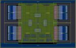
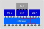
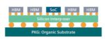
If you have anything to do with the semiconductor industry, you already know that one of the hottest areas for both manufacturing and EDA are systems designed with advanced packaging, basically putting more than one die (aka chiplets) in the same package.
When 3D packaging was first introduced, there were not really any effective… Read More
If, like me, you’ve been paying too little attention to historically less glamorous areas of chip design like packaging, you’ll wake up one day and realize just how much things have changed and continue to advance and how interesting it’s become.
One of the main drivers here is the increasing use of chiplets to counter the decreasing… Read More
I just did a Google search for “3D IC”, and was stunned to see it return a whopping 476,000 results. This topic is trending, because more companies are using advanced IC packaging to meet their requirements, and yet the engineers doing the 3D IC design have new challenges to overcome. One of those challenges is creating… Read More
Our smart phones, tablets, laptops and desktops are the most common consumer products with advanced 2.5D and 3D IC packaging techniques. I love seeing the product tear down articles to learn how advanced packaging techniques are being used, so at the User2User conference in Santa Clara I attended a presentation from Tarek Ramadan,… Read More