Our smart phones, tablets, laptops and desktops are the most common consumer products with advanced 2.5D and 3D IC packaging techniques. I love seeing the product tear down articles to learn how advanced packaging techniques are being used, so at the User2User conference in Santa Clara I attended a presentation from Tarek Ramadan, 3D IC AE at Siemens EDA.

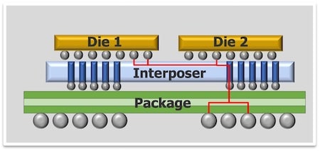
2.5D IC packaging has been accomplished through the use of interposers with silicon or organic substrates, and FO-WLP (Fan-out, Wafer Level Package) is a popular technique. The promise of using chiplets to mix and match IP blocks as dies is another growing trend.


From the design side of things, an engineer wants to know how the connectivity is defined in these packages, plus how to perform a full assembly physical verification to ensure reliability and high yields. A system-level netlist is the goal, and for packaging that uses a silicon interposer it is Verilog, while for an organic substrate CSV is the common description. With different netlist formats, and even different engineering teams, this creates a communication challenge.
Siemens has created something to help these teams work together on packaging, and they call the product Xpedition Substrate Integrator (xSI) which is a tool used for connectivity planning, optimization and management. Engineers can import and export connectivity in lots of formats (Verilog, CSV, ODB++, LEF/DEF, GDS), and also make interactive and manual assignments. The system netlist output can then be used for LVS (Layout Versus Schematic) and STA (Static Timing Analysis) tools.

You can even perform device transformations or scaling, and xSI has the capacity to handle millions of pins. There are four steps in the xSI flow:
- Create a design/floorplan
- Create the different parts
- Align the 3D-IC system
- Apply connectivity to the xSI database
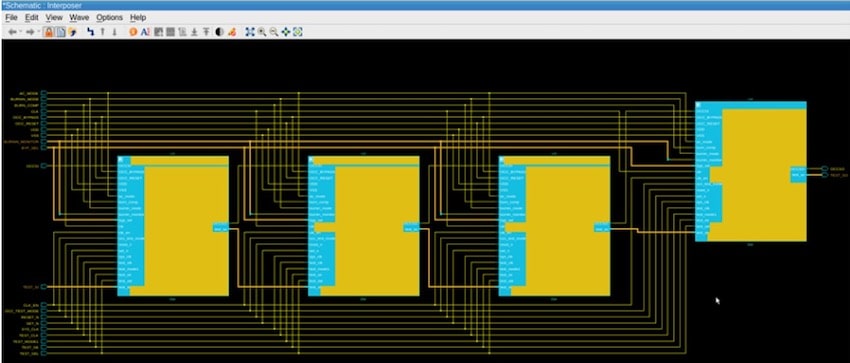
Tarek showed how how parts were created by importing a CSV file, and the example used an interposer with 4 dies and C4, while the package was a BGA and interface C4. The interposer connectivity was defined by Verilog, and then displayed in the Siemens Visualizer Debug Environment.

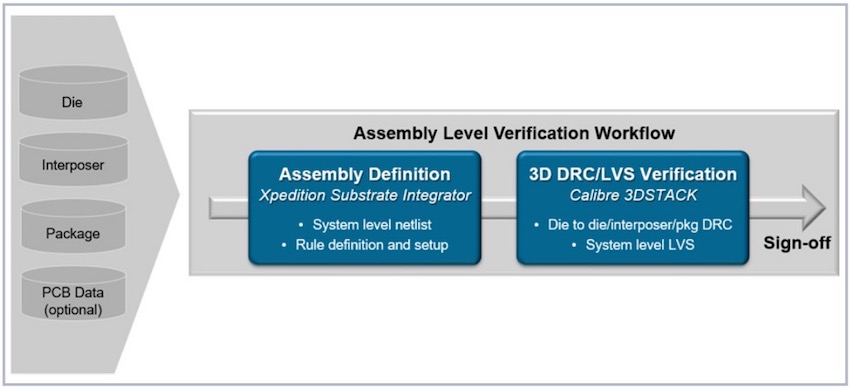
Physical verification DRC and LVS for individual dies and the silicon interposer are performed using the standard PDK supplied from the foundry. An assembly description is really needed for the positioning of each die on the interposer. The Siemens approach is to use both Xpedition Substrate Integrator and Calibre 3DSTACK tools together for assembly level verification.

Q&A
Q: How popular are these tools from Siemens?
A: Since 2017, about 25 customers are using the flow so far. This is really a back-end independent approach. Using both tools in tandem is essential for 3D IC packaging.
Q: Why use an assembly description?
A: It’s the only method to answer the question of where everything is being placed. The assembly can also be checked for consistency.
Q: What about the chiplet association, UCIe?
A: No EDA company was announced at the formation of UCIe, but stay tuned to see EDA companies joining soon. There’s also the Open Compute Platform – CDX chiplet design exchange kit. The UCIe is trying to standardize how chiplets are assembled together.
Summary
Our semiconductor industry has grown the trend of 2.5D and 3D IC by using advanced packaging approaches, and it’s an engineering challenge to properly capture the system-level connectivity. Package engineers and IC engineers use different tools and file formats, so having a tool flow that knows how to combine information from each discipline makes the task of design and verification tenable.
The Siemens tool Xpedition Substrate Integrator has met the needs of 3D IC design challenges, and supporting Verilog for interconnect makes the flow easier to use. On the physical verification side, a 3D IC assembly description is required, and using the combination of xSI and Calibre 3DSTACK ensures that verification is complete.
Related Blogs
- SIP Modules Solve Numerous Scaling Problems – But Introduce New Issues
- Heterogeneous Package Design Challenges for ADAS
- Mentor unpacks LVS and LVL issues around advanced packaging
- High Density Advanced Packaging Trends
- Tools for Advanced Packaging Design Follow Moore’s Law, Too!


Comments
One Reply to “3D IC Update from User2User”
You must register or log in to view/post comments.