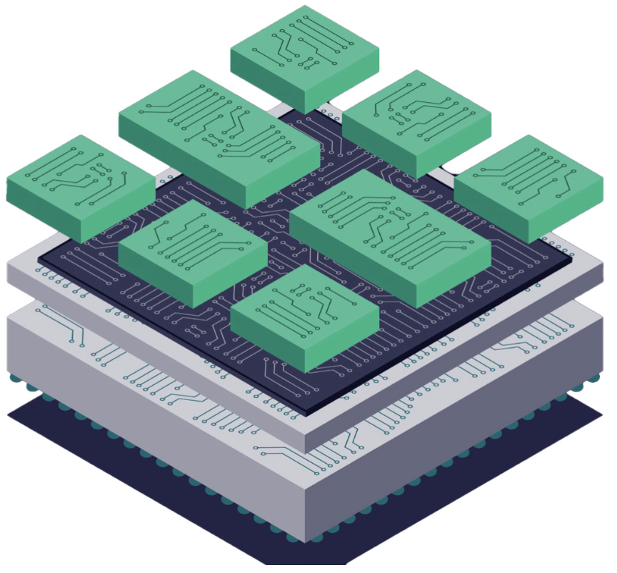


2.5D and 3D ICs present special challenges since these designs contain multiple chiplets of different materials integrated in all three dimensions. This complexity demands full assembly verification of the entire stack, considering all the subtle electrical and physical interactions of the complete system. Identifying the right stack configuration as early as possible in the design process minimizes re-work and significantly improves the chances of success. Siemens Digital Industries Software recently published a comprehensive white paper on how to address these problems. A link is coming, but first let’s examine the array of challenges that are presented in the white paper to see how Siemens EDA makes 3D IC design more accessible with early package assembly verification.
2.5/3D IC Design Challenges
2.5D and 3D ICs are composed of multiple chiplets, each of which may be fabricated on separate process nodes. The white paper talks about some of the challenges for this kind of design methodology. For example, options for connecting chiplets are reviewed. A partial list:
- Chiplets connected via interposer with bump connections and through-silicon-vias (TSVs)
- Chiplets on package
- Chiplets on packages with discreet and thinned interposers embedded without TSVs
- Chiplets stacked on chiplets through direct bonding techniques
- Chiplets stacked on chiplets with TSVs or copper pillars and more bumps
There is a lot to consider.
The 3D IC Assembly Flow
Challenges here include some method to disaggregate the components of a design into appropriate chiplets. Each chiplet must then be assigned to an appropriate foundry technology. The specific approach to assemble the design is critical. Material choices and chiplet placement will induce thermal and mechanical stresses that can impact the intended electrical behavior of the full assembly design. This phase may require many iterations.
3D IC Physical Verification
There are a lot of challenges and new methods discussed in this section. For example, the most common approach for checking physical and electrical compliance for a 3D IC requires the use of separate rule decks for design rule checking (DRC), LVS, etc. for each interface within the package (chip-to-chip, chip-to-interposer, chip-to-package, interposer-to-package, etc.). These rule decks typically use pseudo-devices, commonly in the form of 0-ohm resistors, to identify the connections across each interface while still preserving the individual chiplet-level net names.
Problems here include the fact that designers must associate the many individual rule decks to the corresponding interfaces within the assembly layout, which may not always be intuitive. As errors are identified, designers must be able to highlight them at the proper interfaces (with proper handling of rotations and magnifications) to help identify the appropriate fixes.
Many more challenges are discussed in this section. For example, without a holistic assembly approach, it is impossible to verify ESD protection when the ESD circuits exist in one chip and the protection devices exist in another.
Shift Left IC Design and Verification
In this section, the benefits of a “shift left” or early verification approach are reviewed. Reduced design time and a higher quality result are some of the benefits. How the Calibre nmPlatform and other Siemens EDA tools can be used to implement a shift left approach are discussed.
Shift Left for 3D IC Physical Verification
This section begins by pointing out that 3D IC verification of physical and electrical constraints requires a holistic assembly-level approach. A holistic approach requires full knowledge of both the 3D IC assembly and the individual chiplet processes. Many tools must be integrated in the correct flow and emerging standards such as 3Dblox must be used correctly.
Approaches to handle thermal and mechanical stress analysis are also detailed. This is also a complex process requiring many tools used in the correct way. The importance of a holistic approach is again stressed. For example, thermal and mechanical issues cannot be treated in isolation. Mechanical stresses induce heat. Thermal impacts create mechanical stress, and so on. A correct approach here can avoid unwanted surprises by the time final iteration is performed.
To Learn More
This white paper covers a lot of aspects of package assembly verification for multi-die designs. The benefits of a shift left, or early approach are clearly defined, along with a description of how the current flow must be modified to accommodate these techniques.
If you are considering a multi-die design, I highly recommend reading this white paper. It will save you a lot of time and effort. You can get your copy of this important document here. And that’s how Siemens EDA makes 3D IC design more accessible with early package assembly verification.
Share this post via:


Comments
There are no comments yet.
You must register or log in to view/post comments.