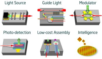

Silicon photonics is one of the upstart “More than Moore” technologies designed to enable the next generation of high-performance devices. Photonic design is the art of moving and transforming signals in the form of photons, allowing the message to literally travel at the speed of light, and bringing the promise of significant performance gains. I’m starting to see evidence that silicon photonics is moving from the research phase into development. The adoption of silicon photonics will be driven by the demands of data center and high-performance computing.
 Another “More than Moore” technology is 3D IC design, in which a design is partitioned into smaller pieces that can be stacked, resulting in smaller form factors and thus allowing more functionality to be packed into tablets and other hand-held devices. Aside from some novel design concepts (such as the memory cube), you will not typically see a performance advantage with 3D designs. In fact, it may degrade performance by introducing longer paths between devices on separate dies.
“As luck would have it,” says John Ferguson, a product marking manager in the Calibre group at Mentor, “silicon surrounded by silicon-oxide makes an almost ideal waveguide material, meaning the optical signals can traverse with very little degradation.” This means that photonics can be designed and manufactured using the same fabs already in place for traditional IC design. Indeed, Intel has already demonstrated this last year when they introduced a 100 Gigabit silicon photonic product (prematurely, it turns out.)
But, of course, there is always a catch. Photonics design is purely passive. If you want to change an optical signal, you must induce that change using either heat or a magnetic field (or both) in the vicinity of the waveguide carrying the signal, says Ferguson. So, just create a design with some photonics components and some electronics components, pass timing-critical data as optical photons and use tried and tested electronics elsewhere, right? Well, maybe not, said Ferguson. If the electrical components are complex, you may need to target those expensive CMOS processes again. Unlike the CMOS transistor, however, there is little benefit in porting a silicon photonic waveguide to an advanced node. That is because the optical behavior for such components is set by the total length and width of the wave guide, along with some other concerns, like bend structures or how close it is to other components. The widths for waveguides in silicon are very large (100-200 nm) compared to today’s CMOS devices. So, even if you go to a new process node, the photonics section stays the same size. Also, Ferguson says, putting photonics on the same die as electronics uses up a lot of expensive silicon real estate for the relatively large photonics structures.
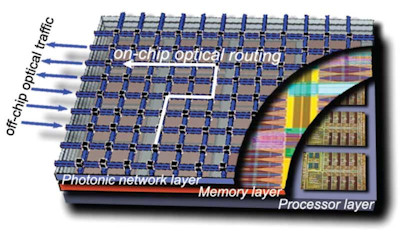 But, you could combine silicon photonic processing with 2.5D processing–partition the optical components to a less expensive process, such as those typically targeted for interposer use (like, say 65nm or 90nm), while targeting those more critical electrical components to a die on a more advanced process node, maybe 28nm. This is where a lot of photonics research is currently targeted. Almost all silicon photonics designers are putting photonics into the interposer itself, which is usually at a more matrure process node like 65nm or 90nm, and then connecting to the electronics as a die on top. In fact, Cisco showed a silicon photonics/2.5D prototype at a 2013 DesignCon keynote. That technology came from Cisco’s 2012 acquisition of optical interconnect company Lightwire.
There are lots of questions to be answered regarding silicon photonics and 2.5 and 3D design. For example, in some designs, like the memory cube, you can actually gain performance by connecting through a TSV, but it requires careful die to die placement such that the critical devices on either side are close to the TSV, says Ferguson. In such a case, you can have an electrically closer signal. Usually this means stacking directly on top of the signals in question. Unfortunately, outside of the memory world, so far this approach typically fails due to thermal impact. An active die with lots of switching can produce a lot of heat. Setting it on top of another active die can cause problems for the neighboring die devices. This problem is even more concerning to the photonics design because heat will change the behavior of the optical signals through the wave guide Fortunately, we’ve already learned to stack them like a stair case, Ferguson says, where the interposer juts out from the die and in the extruding area the photonics are inserted. Doing this in the less expensive interposer is far less costly than folding it all into the same expensive advanced-node die.
What impact will this have on the photonics components? The photonics will require a laser source, but because we’ve yet to produce a usable silicon laser in standard CMOS process, it will need to sit off-die. What impact will this have on the form-factor? What impact will the heat generated by the laser have on the near-by electronic components?
Is there was a way around the limitations imposed by TSVs? Oh, say, with photonics? Because light signals can pass through each other essentially unimpeded, this also brings the theoretical ability to eliminate the need for vias, dramatically reducing the power required to pass said signal. There is some high-level research in this area, but nothing practical yet.
There is a lot of work to do, and silicon photonics is a dynamic industry. A major hint that this is big-time interesting is that the government set up a National Photonics Initiative in 2013 and seeded it with $200 million. In the private sector, start-up Luxtera uses CMOS photonics to get around limitations of electrical chip I/O bandwidth. Another silicon photonics start-up, Kotura, was swallowed up by Mellanox in 2013. ST Microelectronics and Infinera are also active in the field. The global silicon photonics market is projected to grow from about $25 million in 2013 to between $400 and $500 million by 2020. And while it is exciting to think of what silicon photonics will do for our data centers, it also promises equally exciting advances in powerful and compact chemical and biological sensors.
Share this post via:


Comments
0 Replies to “Why silicon photonics and 2.5D design go together”
You must register or log in to view/post comments.