
How do you ensure your design has been optimized for power, performance, and area? I posed this question to Mentor’s Group Director of Marketing, Sudhakar Jilla and product specialist Mark Le. They said that finding the PPA sweet spot is still often done by trial and error – basically serial experiments with various input parameters… Read More

Author: Beth Martin
How to nail your PPA tradeoffs

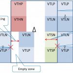
Low power physical design in the age of FinFETs

Low power is now a goal for most digital circuit designs. This is to reduce costs for packaging, cooling, and electricity; to increase battery life; and to improve performance without overheating. I talked to the experts on physical design for ultra-low power at Mentor Graphics recently about the challenges to P&R tools and… Read More
A new world of 10nm design constraints
Every time the industry transitions to a smaller process node IC design software undergoes extensive updates.
I talked to a couple of experts in physical design at Mentor Graphics about what is involved in making place-and-route software ready for a new node. This is what I learned from Sudhakar Jilla, the IC design marketing director… Read More
Price of Admission $0.00 at Inaugural Silicon Valley Conference

Back in 2002, the Southwest DFT Conference was born and experts on design for test (DFT) and test got together to share ideas and talk to people in this industry that were trying to solve test challenges of the day.… Read More
What’s Testing Design Limits at ITC?

The 46[SUP]th[/SUP] IEEE International Test Conference (ITC) will be held the week of October 5, 2015 at the Disneyland Hotel Conference Center in Anaheim, California. ITC is where you will discover the latest ideas and learn about practical applications of test technologies.
As you take in panels, tutorials, presentations,… Read More
Together At Last—Combining Netlist and Layout Data for Power-Aware Verification

The market demanded that gadgets it loves become ever more conscious of their power consumption, and chip designers responded with an array of clever techniques to cut IC power use. Unsurprisingly, these new techniques added to the complexity of IC verification. When you’re verifying a design that has 100+ separate power domains,… Read More
For high-volume manufacturing at 10 nm and below: technology and friendship
The technology for 10 nm is settled, but what about 7 nm and 5 nm? Those nodes will happen with silicon-based CMOS and 193nm immersion lithography, but exactly how is still being worked out. Right now, though, the focus is on getting 10 nm chips into high-volume production. TSMC and Intel both claim to be on track for high-volume manufacturing… Read More
Test Driving Analog/Mixed Signal Design for the Internet of Things

The Internet of Things (IoT) is creating urgent demand for a new generation of analog/mixed-signal (AMS) designs, some of which also contain MEMs. To efficiently create the myriad of AMS devices at the edge of the IoT requires a design environment that is affordable and easy to use, but powerful enough to create the widely diverse… Read More
Addressing Moore’s Law with the First Law of Real Estate: Location, location, location

Design sizes and complexities have grown exponentially (it’s a Law!), and consequentially the task of silicon test has become proportionally more expensive. The cost of testing a device is proportional to the amount of test data that is applied, and therefore the time it takes, which in turn is proportional to both design size … Read More
Boost the Market for Interposer and 3D ICs with Assembly Design Kits

The traditional system-on-chip (SoC) design process has fully qualified verification methods embodied in the form of process design kits (PDKs). Why is it that chip design companies and assembly houses have no IC/package co-design sign-off verification process?
Package die are often produced using multiple processes and… Read More


TSMC CoWoS versus Intel EMIB Semiconductor Packaging