Design sizes and complexities have grown exponentially (it’s a Law!), and consequentially the task of silicon test has become proportionally more expensive. The cost of testing a device is proportional to the amount of test data that is applied, and therefore the time it takes, which in turn is proportional to both design size and the number of defect types that need to be covered.
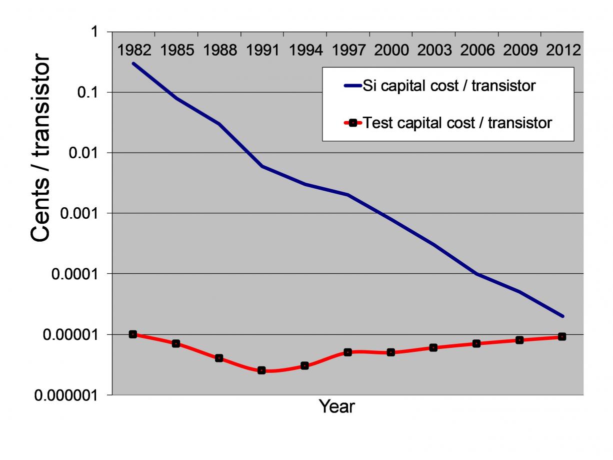
ATPG (automatic test pattern generation) had to become much more efficient in order for test costs to remain economical. It became painfully clear by the year 2000 that within a decade, it would cost more to test each transistor than to manufacture it. Figure 1 shows the cost/transistor trend of manufacturing and test.

This powerful need for more economical test drove the development of ATPG compression technology. While the amount of compression has improved over the years, new factors like more complex design structures and the need to cover more advanced fault types like Cell-Aware faults are driving the need for compression levels beyond what is typically achievable even with the most advanced compression solutions.
I talked to Steve Pateras, product marketing director for Mentor Graphics Silicon Test Solutions, about an extremely promising new approach to reducing ATPG pattern volume using a novel type of test point technology. Pateras said that the reduction in ATPG pattern volume when these EDT (embedded deterministic test) test points are inserted into the design depends on the number of test points used and the design characteristics, but empirical results have shown significant reductions, typically in the 2X to 4X range. Combining the use of these test points with ATPG compression can therefore improve overall compression levels from a typical 100X to as much 400X or more. This level of test pattern reduction results in real time and cost savings, and is a compelling value proposition.
About ATPG Compression
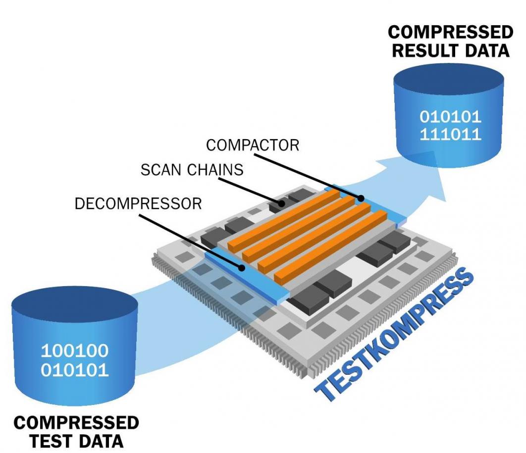
But first, some background. With ATPG compression, on-chip circuitry is added to intercept and decompress test patterns before streaming into the device’s scan chains. Only the compressed test data is stored on the external tester and applied to chip pins (Figure 2).

On-chip logic is also added on the output of the scan chains to compact the test responses before unloading back to the tester. ATPG compression reduces both test data volume and test application time. You want to reduce data volume to limit ATE memory requirements and related costs. In particular, you want to ensure that all test patterns can fit into the tester’s existing memory, since it’s expensive to reload the tester with additional patterns at each device insertion. Reducing test time is important too because test time is directly correlated to test cost per device. Leading edge ATPG compression technology can generally achieve 100X compression.
Despite these drastic ATPG improvements over the years, test pattern volumes continue to increase along with the increasing design sizes. The challenge is to reduce test pattern volumes without losing test quality. This is where EDT test points come in.
About EDT Test Points
Here is how Pateras explained test points to me: Test points consist of local modifications to the netlist designed to increase the controllability or observability of a given net. Test points have been used for years in conjunction with logic BIST to reduce the number of random patterns needed to achieve an acceptable level of fault coverage. The test points were inserted in locations that would maximize the random pattern testability of the circuit under test.
EDT Test Points consist of the same local modifications, but the similarity with logic BIST test points ends there. Just like in real estate, Pateras said, location is absolutely everything. The test geniuses at Mentor developed an innovative selection algorithm to choose the location of test points that would maximize deterministic pattern reduction.
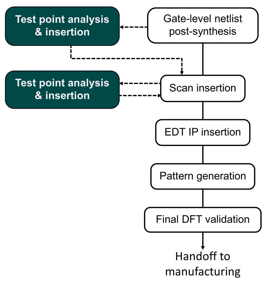
ATPG software models a fault in the logic, then traces a path back to the input to control the data to simulate the fault, then propagates the effects of the fault to an output. By adding test points at strategic locations, the pattern generation becomes more efficient, runs faster and creates fewer patterns. To insert test points, Mentor’s software (Tessent ScanPro) analyzes the netlist, either before or after scan insertion, and determines the optimum number and locations for test point insertion. The rest of the ATPG flow, shown in Figure 3, remains unchanged.

I asked Pateras what effect the insertion of test points has on timing and power. It is generally limited, he said, because physical synthesis should optimize away any timing impacts. However, to mitigate any impact on timing closure, he said critical paths extracted from static timing analysis can be excluded from test point insertion. The number of control points added to a single path can also be limited. The overall number of control versus observe points can also be controlled to favor the more timing-neutral observe points if necessary.
Empirical Results
The EDT Test Point technology has been used in many designs so Mentor has a large amount of empirical data. The amount of pattern reduction you get is, in general, proportional to the number of EDT Test Points added to the design. This trade-off is illustrated in Table 1. Even a small number of EDT Test Points, say only 0.15% area overhead, will typically provide an almost 2X pattern reduction.
You can read more about EDT Test Points in this Mentor whitepaper.
Share this post via:


Comments
There are no comments yet.
You must register or log in to view/post comments.