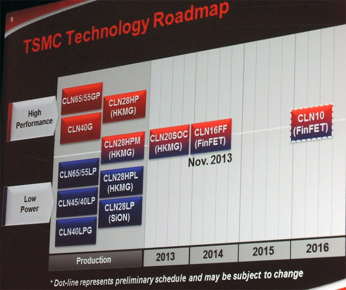
The technology for 10 nm is settled, but what about 7 nm and 5 nm? Those nodes will happen with silicon-based CMOS and 193nm immersion lithography, but exactly how is still being worked out. Right now, though, the focus is on getting 10 nm chips into high-volume production. TSMC and Intel both claim to be on track for high-volume manufacturing (HVM) of 10 nm FinFET processors by 2017. You can see in the image below that it is a real “dotted-line” prediction.
Achieving HVM past 14 nm and getting to 5 nm was the topic of a panel session at this year’s SemiconWest. I talked to panelist Juan Rey, senior engineering director at Mentor Graphics, about EDA’s role in the march to the ‘Last Node Ever.’
Meaningful discussions of process nodes must include viewpoints from all niches of the semiconductor ecosystem. This panel included experts from IMEC (semi process research), Soitec (semiconductor materials), Intermolecular (materials, process, HVM), LAM (fab equipment), Applied Materials (fab equipment), and Mentor Graphics (EDA).
An early question to the panelists was about the options for improving devices. An Steegen from IMEC talked about some recent R&D areas, including SiGe and GeAs high-mobility channels, under-etching, bi-layer graphene, and vertical silicon nanowires. Those silicon nanowires are also called gate-all-around transistors, and are a likely replacement to today’s FinFETS at 7 nm and 5 nm.
Christophe Maleville of Soitec focused on FDSOI as a path to HVM for 10 nm. The materials and equipment panelists talked about atomic-level etch and deposition, and also about improvements in scanning electron microscopy (SEM) used for metrology. Being an EDA person, the materials discussions were fascinating to me, but a little out of my wheelhouse. However, I suspect I’ll be learning more about these emerging technologies, particularly the gate-all-around transistors.
The final panelist in the session was Juan Rey from Mentor Graphics, who talked about the challenges at the interface of design and manufacturing. That ever-shifting borderland is where Rey spends most of his time. While Mentor’s work is highly technical, he started with a higher-level discussion about the need for better communication through the ecosystem. He says that the iterations between foundries and their partners must happen sooner, and in smaller, faster cycles. That is, the path to HVM will be accelerated when there is tighter cooperation between EDA, IP providers, and foundries.
He also suggested that foundries need to restrict the number of partners they engage with, so they can form deeper relationships with fewer key partners. On the more technical side, Rey said that EDA companies constantly work on multiple enabling technologies without always knowing which one will work, or which one will be widely adopted. Mentor, for example, has software for directed self-assembly (DSA), EUV, multi-patterning (both SADP and LELE), etc.
Take physical verification, for instance. The chart shows the proliferation of technology for physical verification by node. Each technology was developed to address specific challenges to design and manufacturing; lithography limitations required resolution and mask enhancements, planarity and loading effects called for new fill methods, FinFETS needed whole new device and interconnect models, and so on.
Integration between tools is also important, said Rey. He used examples of how Calibre verification based on sign-off foundry decks are interfaced with all major digital place and route tools and custom design tools. These tight interfaces improve the design flow productivity, particularly for multi-patterning, by essentially dropping the full Calibre signoff capabilities into the design and edit environment. This type of tight integration between tools can make a big difference in design productivity.
For more on productivity improvements through better tool interactions, you can download a free whitepaper on STMicroelectronic’s experience using Calibre RealTime on a 14nm FDSOI design.
Another issue Rey discussed is encryption to protect foundry IP. The problem is that EDA tools need lots of information on IP to generate accurate verification results, but the foundries are reluctant to provide such sensitive IP information in rule decks. The solution, says Rey, is partial deck encryption. This makes the foundry’s sensitive IP information unreadable to humans, but perfectly clear to the EDA tools.
The take-away from these experts overall is that there *is* a clear path to HVM for 10 nm, and a somewhat more winding and ambiguous path to 5 nm. The panelists didn’t seem discouraged, but excited about figuring out the solutions to the challenges that lay ahead.
Share this post via:


Comments
0 Replies to “For high-volume manufacturing at 10 nm and below: technology and friendship”
You must register or log in to view/post comments.