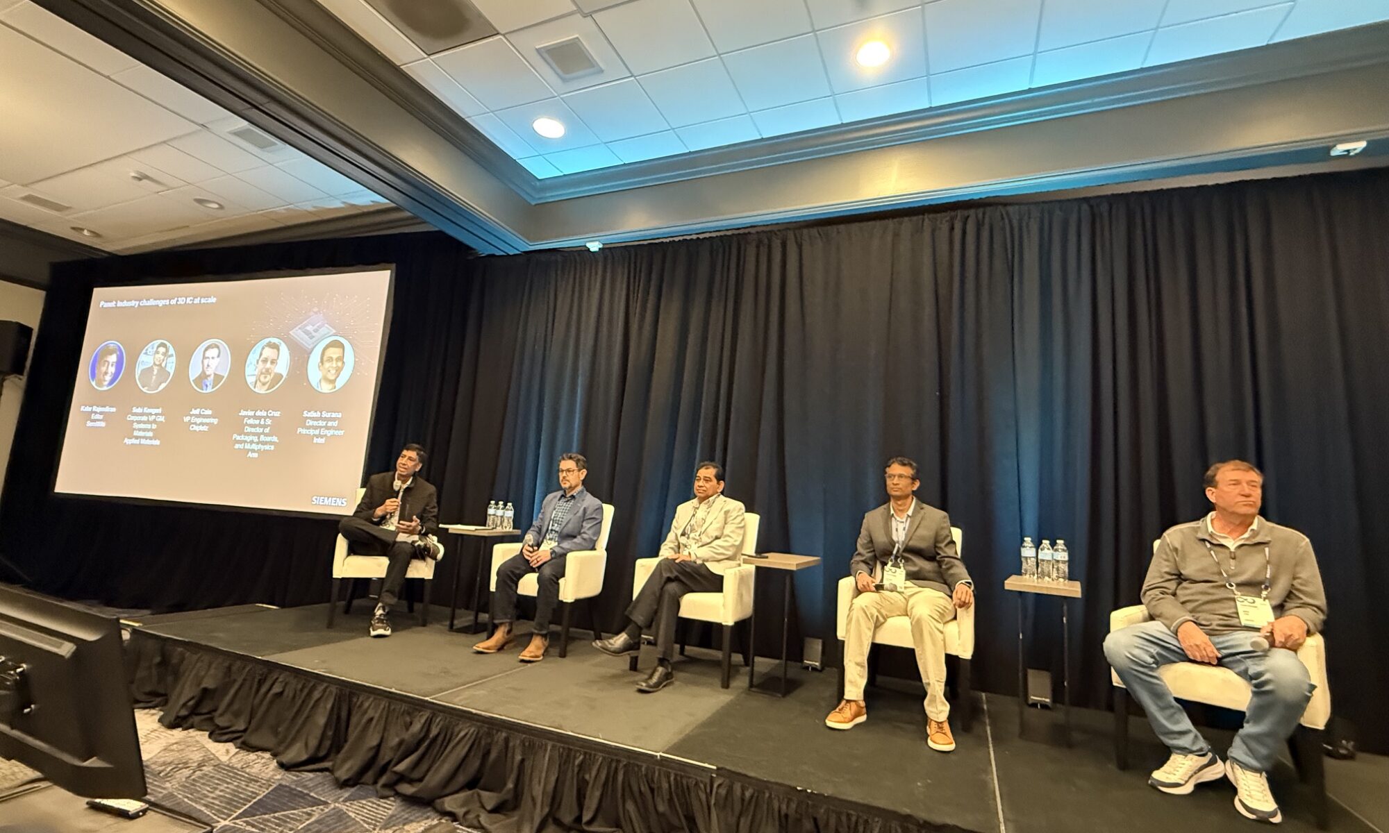


Given the success of the event in Silicon Valley last week, I would expect the Siemens U2U event in Munich to be even bigger. In my experience this has been the best user driven event in 2026 with the deepest customer content. EDA has always been a customer driven industry and it is good to see us recognize that from time to time. Kalar was the moderator on this panel so I was in the front row taking notes.
The semiconductor industry is entering a pivotal phase as it transitions from traditional 2D ICs to 3D ICs and chiplet-based architectures. This shift represents a fundamental evolution in how chips are designed, manufactured, and deployed. Rather than relying solely on shrinking transistors, engineers are now stacking and integrating multiple dies into a single package, enabling higher performance, better power efficiency, and greater system flexibility. While this approach unlocks significant advantages, it also introduces a new set of challenges that must be addressed for widespread adoption.
At its core, 3D integration allows different functional components, such as logic, memory, and accelerators, to be combined in a modular fashion. This enables scalable architectures and significantly improves bandwidth by reducing the distance data must travel between components. It also allows designers to mix and match technologies from different process nodes, optimizing each function independently. As a result, 3D ICs are becoming essential for applications like artificial intelligence, high-performance computing, and data centers, where performance and efficiency are critical.
However, the move to 3D scaling is far from straightforward. One of the most significant challenges is the increased complexity across the entire development lifecycle. In traditional chip design, many issues could be addressed at the component level. In contrast, 3D ICs require a system-level perspective, where interactions between dies, packaging, and the overall system must be carefully managed. Thermal and power considerations, in particular, have become major concerns. As power density increases, heat dissipation becomes more difficult, and inefficient power delivery can lead to both performance limitations and reliability issues.
Another critical challenge is supply chain and manufacturing capacity. The semiconductor industry has experienced rapid growth, with demand accelerating at an unprecedented rate. While this growth is positive, it has also exposed limitations in infrastructure. Building new fabrication facilities and expanding cleanroom capacity takes years, and advanced packaging processes are becoming increasingly complex. Technologies such as hybrid bonding, high-bandwidth memory integration, and large interposers require sophisticated equipment and processes that are not yet widely available. These constraints can create bottlenecks, particularly for smaller companies trying to enter the market.
To navigate these challenges, industry experts emphasize the importance of early architectural planning. In the past, packaging was often treated as a secondary consideration, addressed after the core chip design was complete. This approach is no longer viable. Advanced packaging must now be considered at the very beginning of the design process, alongside system architecture and functionality. Decisions about packaging technology, supply chain partners, and manufacturing processes must be made early to avoid costly redesigns and delays. Designing for manufacturability and yield is especially important, as even small inefficiencies can significantly impact production capacity and cost.
Interoperability and standardization are also key factors in enabling the growth of the 3D IC ecosystem. Efforts to develop open standards for die-to-die communication aim to make it easier to integrate components from different vendors. While these standards can reduce barriers to entry and promote innovation, they are not a complete solution. In practice, achieving seamless interoperability is challenging due to differences in design choices, protocols, and performance requirements. As a result, many high-performance systems still rely on customized interfaces to achieve optimal results, while standards play a more prominent role in mid-range and emerging applications.
Looking ahead, innovation in materials, cooling, and power delivery will be essential to overcoming current limitations. New substrate materials, such as glass, offer improved mechanical stability and finer feature resolution compared to traditional organic substrates. Advanced cooling techniques, including near-chip cooling and novel heat dissipation methods, are being explored to manage increasing thermal loads. Similarly, improvements in power delivery, such as backside power distribution and integrated voltage regulation, are critical for supporting the high current densities required by modern systems.
Another promising area of development is the use of advanced modeling and simulation tools. Multiphysics simulation, which accounts for electrical, thermal, and mechanical interactions, is becoming increasingly important in 3D IC design. By incorporating these analyses early in the design process, engineers can identify potential issues and optimize system performance before manufacturing. Digital twin technology, which creates a virtual representation of the entire system and manufacturing process, is expected to play a major role in improving design accuracy and reducing time to market.
Bottom line: The transition to 3D ICs and chiplet architectures marks a significant turning point in semiconductor innovation. While the benefits in performance, efficiency, and flexibility are substantial, the challenges are equally complex. Success in this new era requires a holistic approach that integrates design, manufacturing, and system considerations from the outset. By investing in early planning, embracing new technologies, and fostering collaboration across the ecosystem, the industry can overcome these challenges and unlock the full potential of 3D integration.
MUNICH, GERMANY | MAY 12, 2026 User2User Europe
Also Read:
Solving the EDA tool fragmentation crisis
Exploring the Hidden Complexity of Modern Power Electronics Design – A Siemens White Paper
Siemens Wins Best in Show Award at Chiplet Summit and Targets Broad 3D IC Design Enablement
Share this post via:


Comments
One Reply to “Siemens U2U 3D IC Design and Verification Panel”
You must register or log in to view/post comments.