

The semiconductor industry has spent decades optimizing tools. Today, however, the central challenge is no longer whether individual tools are powerful enough. The real question is whether increasingly specialized tools, domains, models, and organizations can still converge coherently into a manufacturable, reliable, high-performance system.
That distinction matters.
Recent discussions around interoperability frameworks such as Siemens’ Calibre Connectivity Interface (CCI) highlight an important and necessary evolution in the industry. By transforming LVS verification output into a structured, queryable data foundation for downstream tools, the industry is moving beyond isolated verification flows toward connected engineering ecosystems. This is a major step forward. But interoperability alone does not guarantee system-level convergence. That distinction is becoming increasingly important as semiconductor systems move from tool-limited complexity to convergence-limited complexity, as illustrated in Figure 1.

At advanced nodes, particularly below 5nm and within heterogeneous integration architectures, fragmentation is no longer limited to tools alone. It now spans abstraction layers, physics domains, organizations, manufacturing flows, packaging ecosystems, and even decision authority itself. Modern system realization extends across architecture, silicon, package, interposer, PCB, thermal, mechanical, SI/PI, electromagnetic behavior, reliability, validation, and manufacturing integration. Each of these domains is represented by highly specialized tools that are often locally optimized but globally disconnected.
This creates a dangerous illusion: every domain can appear “correct” while the overall system still fails to converge.
The industry is beginning to encounter what can be described as a convergence scaling crisis.
As systems become more tightly coupled, the number of interactions between engineering domains grows nonlinearly. At some point, organizations encounter an “Entropy Wall,” where the complexity of cross-domain coordination grows faster than the organization’s ability to reason about it coherently. Historically, engineering scale was constrained by transistor count, lithography, frequency, or power density. Increasingly, the limiting factor is becoming convergence capacity itself. In other words, the industry may not be running out of compute capability nearly as quickly as it is running out of governed decision-making capability.
Many organizations assume that AI will naturally resolve this fragmentation. In practice, however, uncontrolled AI risks amplifying fragmentation rather than reducing it. Most engineering environments already operate with conflicting models, inconsistent assumptions, disconnected evidence chains, isolated optimization loops, tool-specific abstractions, and incomplete causality tracking. AI systems trained across such fragmented ecosystems can accelerate local optimization while simultaneously increasing global instability.
This highlights a critical distinction: intelligence is not convergence. Prediction is not governance. Automation is not authority.
The next architectural transition therefore extends beyond interoperability toward what can be described as governed convergence. Interoperability ensures that tools can exchange information, but governed convergence ensures that fragmented engineering evidence can be normalized, causally bounded, and used to drive deterministic system-level decisions.
This distinction becomes especially important in chiplet ecosystems, advanced packaging, 2.5D and 3D integration, AI accelerator platforms, high-speed interconnect architectures, and multi-vendor manufacturing environments. In these systems, the challenge is no longer simply moving data between tools. The challenge is orchestrating convergence across the entire engineering stack.
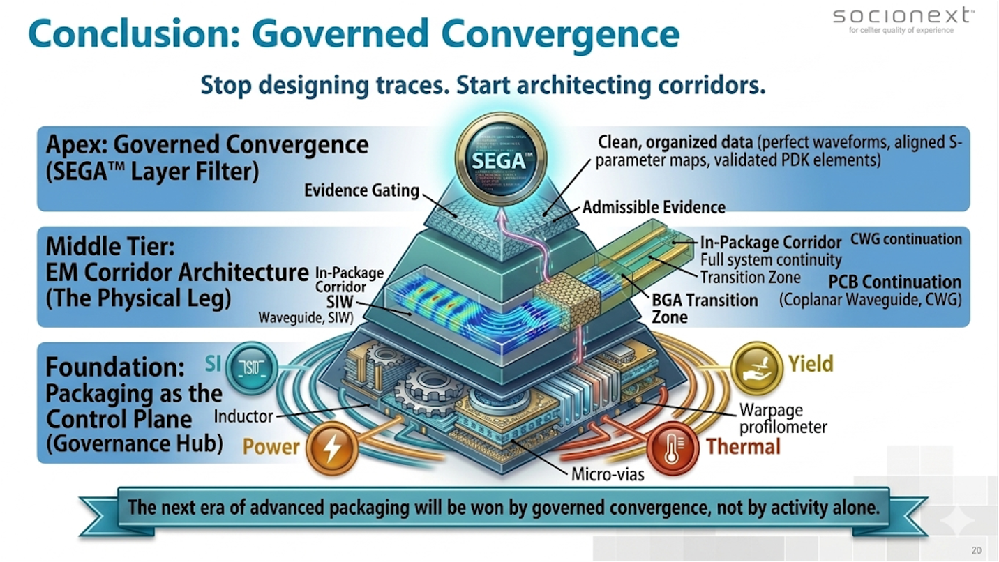
Historically, packaging has been treated primarily as a physical integration layer. That assumption is rapidly changing. At multi-terabit bandwidths and in highly coupled heterogeneous systems, packaging increasingly functions as an active control plane through which power integrity, thermal behavior, signal integrity, manufacturability, and system stability must converge simultaneously. The package is no longer merely carrying the system; it is increasingly governing the system.
One of the least discussed realities in advanced semiconductor development is that governed convergence capacity itself is becoming scarce. The industry already possesses exceptional domain expertise, powerful simulation environments, advanced AI techniques, and enormous compute capability. What remains limited is the ability to coordinate these domains coherently, preserve authoritative evidence, bound uncertainty, and make deterministic cross-domain decisions at scale.
This is fundamentally an orchestration challenge.
Not merely a compute challenge. Not merely a tool challenge. And not merely an AI challenge.
The work being done around interoperable verification ecosystems is therefore extremely important because it establishes the foundation for this next stage. The ability to create trusted, queryable, authoritative engineering evidence layers is a prerequisite for any future convergence architecture.
However, as systems continue to scale in complexity, the industry may increasingly require governance architectures, orchestration frameworks, evidence-driven gate systems, and bounded AI-assisted convergence engines capable of operating across fragmented engineering ecosystems without losing determinism, traceability, or accountability.
The semiconductor industry has solved scaling through abstraction many times before.
The next scaling problem may be convergence itself.
By Dr. Moh Kolbehdari
Dr. Moh Kolbehdari is a Senior Lead Architect at Socionext, where he specializes in the industrialization of high-performance AI chiplets and 1.8-Tb/s interconnects. With over two decades of experience in SI/PI, electromagnetic field theory, and system-level architecture, he has been a pivotal force in bridging the gap between cutting-edge silicon design and high-volume manufacturing (HVM).
Dr. Moh is the creator of the SEGA™ (Systematic Engineering Governance Architecture) framework, a methodology designed to solve the “Crisis of Complexity” in heterogeneous integration. His work focuses on transforming the package into an Active Control Plane, utilizing field-confined EM Corridors and state-aware causality to ensure deterministic yield at 2nm and beyond. He is a frequent contributor to industry-standard committees and is recognized for his “Physics-First” approach to solving the semiconductor industry’s most challenging entropy walls.
Also Read:
Solving the EDA tool fragmentation crisis
Carbon in the Age of AI Chips: What the Semiconductor Industry Needs to Know This Earth Day
Speculation: Silicon’s Most Expensive Compulsion
Share this post via:


Consolidation and Competition: Who is Winning the $4.5 Billion Interface IP Race?