You are currently viewing SemiWiki as a guest which gives you limited access to the site. To view blog comments and experience other SemiWiki features you must be a registered member. Registration is fast, simple, and absolutely free so please,
join our community today!
Before EDA becomes AI-native, focused agents have a window to prove measurable engineering value inside existing design flows.
AI is entering semiconductor engineering from several directions at once.
Some companies are building broad agentic design environments. Others are attacking specific bottlenecks: timing closure,… Read More
AI can compress the path to tape-out. The next challenge is compressing physical realization.
Something important is beginning to happen in semiconductor development: the design cycle itself is becoming compressible.
AI-assisted engineering can accelerate architecture exploration, RTL development, verification, physical… Read More
AI may close the design. The fab may finish the silicon. Production still has to realize the system.
Semiconductor engineering is becoming extraordinarily capable.
EDA platforms are expanding from individual design tasks toward increasingly complete system analysis.
Multiphysics simulation is connecting electrical, … Read More
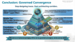
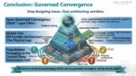
Advanced semiconductor systems are no longer limited by a single engineering domain. They are constrained by the convergence of many interdependent vectors: silicon nodes, advanced packaging architectures, substrate materials, platform PCBs, power-delivery networks, thermal behavior, manufacturing variation, firmware… Read More
The semiconductor industry has spent decades optimizing tools. Today, however, the central challenge is no longer whether individual tools are powerful enough. The real question is whether increasingly specialized tools, domains, models, and organizations can still converge coherently into a manufacturable, reliable,… Read More
Dr. Moh Kolbehdari is a Senior Lead Architect at Socionext, where he specializes in the industrialization of high-performance AI chiplets and 1.8-Tb/s interconnects. With over two decades of experience in SI/PI, electromagnetic field theory, and system-level architecture, he has been a pivotal force in bridging the gap between… Read More