







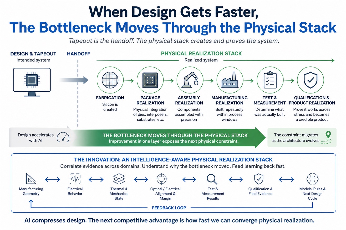
AI can compress the path to tape-out. The next challenge is compressing physical realization.
Something important is beginning to happen in semiconductor development: the design cycle itself is becoming compressible.
AI-assisted engineering can accelerate architecture exploration, RTL development, verification, physical implementation, optimization, and debug. As design-to-tape-out cycles shrink, activities that once consumed a large fraction of a semiconductor program may take less time.
That is a major engineering achievement.
But it creates another question:
What becomes the bottleneck when design gets much faster?
The bottleneck does not disappear.
It moves.
And increasingly, it moves into and through the physical realization stack.
Tape-out Is the Handoff, Not the Physical Stack
Tape-out completes the design representation that fabrication will attempt to realize.
After tape-out, the problem changes.
The intended design has to become silicon. The silicon has to become an integrated package. The required electrical, thermal, mechanical, and increasingly optical physics have to survive real geometry. Assembly has to reproduce that geometry within useful tolerances. Manufacturing has to create it repeatedly. Test has to determine what was actually built. Qualification has to establish whether the resulting system remains functional across stress and operating conditions.
The physical realization stack can therefore be viewed as:
fabrication → package realization → assembly realization → manufacturing realization → test & qualification → product realization
The distinction is fundamental:
Design and tape-out describe the intended system.
The physical realization stack creates and proves the realized system.
As AI compresses design and tape-out, the bottleneck increasingly migrates into and through this physical stack.
The Bottleneck Becomes Distributed Across the Physical Stack
There may no longer be one permanent semiconductor bottleneck.
The constraint moves as architecture changes.
Increase compute capability and memory bandwidth may become limiting.
Move more HBM closer to compute and the bottleneck can shift toward package density, power delivery, thermal gradients, warpage, and assembly.
Improve electrical I/O and electrical reach becomes increasingly difficult.
Move optical conversion closer to compute and electrical distance becomes shorter, while optical alignment, thermal exposure, package stress, fiber attachment, test access, and manufacturing tolerance become more important.
Increase system density further and the bottleneck can move again into cooling, power conversion, optical fabrics, or infrastructure.
The bottleneck moves through the physical stack.
Improvement in one layer often exposes the next physical constraint.
The result is a distributed bottleneck whose location changes as the architecture evolves.
Physical Realization Is Part of the Bottleneck Stack
Physical realization is sometimes treated as what happens after the important design work is finished.
For advanced heterogeneous systems, that view is increasingly difficult to maintain.
A transmitter can be correct.
A receiver can be correct.
A nominal interconnect can pass simulation.
Yet actual margin can still depend on bump height, reference geometry, substrate variation, assembly alignment, warpage, temperature, and mechanical movement.
The intended physics has to survive the realized geometry.
The same principle applies elsewhere.
A high-conductivity thermal material can underperform because of bond-line thickness, contact resistance, pressure, voiding, or warpage.
A photonic device can demonstrate excellent optical performance while package stress, alignment variation, thermal drift, fiber attachment, calibration, or test access limits the product.
A power-delivery architecture can work nominally while package geometry and temperature change resistance, inductance, current distribution, and thermal behavior.
Physical realization is therefore not simply another schedule item.
It is one of the places where the bottleneck itself can reside.
Packaging Moves Toward the Center of the Physical Bottleneck Stack
Advanced packaging increasingly determines how multiple physical domains meet.
It connects compute to memory.
It creates electrical transport geometry.
It distributes power.
It establishes thermal paths.
It constrains mechanical movement.
It increasingly carries optical interfaces.
And it establishes many of the manufacturing and test boundaries through which those functions must pass.
Packaging therefore sits near the center of the physical bottleneck stack.
This does not mean packaging is always the bottleneck.
It means packaging is increasingly where several possible bottlenecks intersect.
That makes package architecture important not only for integration density, but for determining whether improvements elsewhere in the system survive physical implementation.
The Innovation: An Intelligence-Aware Physical Realization Stack
The next step is not simply AI in packaging, AI in test, AI in manufacturing, or AI in reliability as separate applications.
The larger opportunity is an intelligence-aware physical realization stack.
The contribution proposed here is a shift from isolated downstream automation toward intelligence that follows the physical product across realization.
Manufacturing, metrology, electrical, thermal, mechanical, optical, test, qualification, and eventually field evidence should increasingly be correlated around the same realized system.
That creates relationships such as:
manufacturing geometry → electrical behavior
assembly conditions → package warpage
warpage → interface margin
thermal state → mechanical movement
mechanical movement → optical or electrical shift
qualification results → updated process windows
measured hardware → improved models and design rules
The goal is not merely to make every activity faster.
It is to identify where the bottleneck has moved, understand why it moved, connect the evidence needed to act on it, and return that learning upstream fast enough to accelerate the next realization cycle.
The loop becomes:
design → build → measure → correlate → learn → improve
This is an important gap in much of today’s AI discussion.
AI is advancing rapidly upstream, where design information is largely digital and structured.
The physical realization stack produces a different class of evidence: geometry, process history, electrical measurements, thermal behavior, mechanical movement, optical performance, qualification results, and field observations.
Connecting those forms of evidence is more difficult.
But that is precisely where intelligence can become more valuable than isolated automation.
The Next Compression Problem
If design-to-tape-out time falls while fabrication, package realization, assembly, manufacturing learning, test, and qualification remain relatively fixed, those stages become a larger share of the total development cycle.
The bottleneck moves downstream and then continues moving through the physical stack.
The next major opportunity is therefore not only faster design.
It is to make the physical realization stack converge faster.
That requires more than independent automation inside each engineering domain.
It requires stronger connection between the physics we intend, the structures we manufacture, the behavior we measure, and the evidence we feed back into engineering.
The question for the next generation of semiconductor development may therefore become:
How quickly can we identify, understand, and move the bottleneck through the physical realization stack—from intended physics to a repeatable, qualified product?
AI is beginning to compress design.
The larger opportunity is to compress physical realization.
The bottleneck will keep moving. The winning engineering system will be the one that can move with it.
Also Read:
The Fab Is Not the Finish Line
Temperature Does Not Only Age Hardware — It Moves the System
From Photonics Precision to Repeatable Evidence
Share this post via:




Terafab’s Single Roof: Why Packaging, Not Lithography, Decides High Volume