





At the 2026 OIP Ecosystem Forum, the industry narrative shifted from incremental scaling to what TSMC defines as the “Intelligence Revolution.” Akin to the 18th-century Industrial Revolution which transitioned human physical labor to mechanical power, the current era is augmenting human ingenuity through artificial intelligence. We are seeing the birth of workload-specific architectures where AI and human creativity operate in a continuous, high-performance feedback loop.
More Than Two Decades of Collaboration: The OIP Foundation
The Open Innovation Platform (OIP) has matured over twenty years from a standard design-center initiative into the industry’s most formidable collaborative engine. What began as a nascent effort to simplify the path to silicon has expanded into a 90-member powerhouse across six specialized alliances: the Design Center Alliance (DCA), EDA Alliance, IP Alliance, Cloud Alliance, VCA Alliance, and the 3DFabric Alliance.
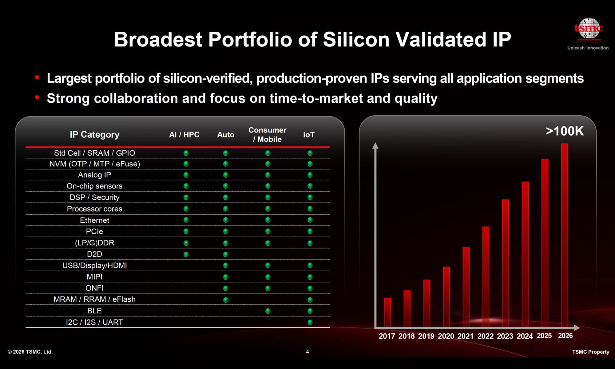
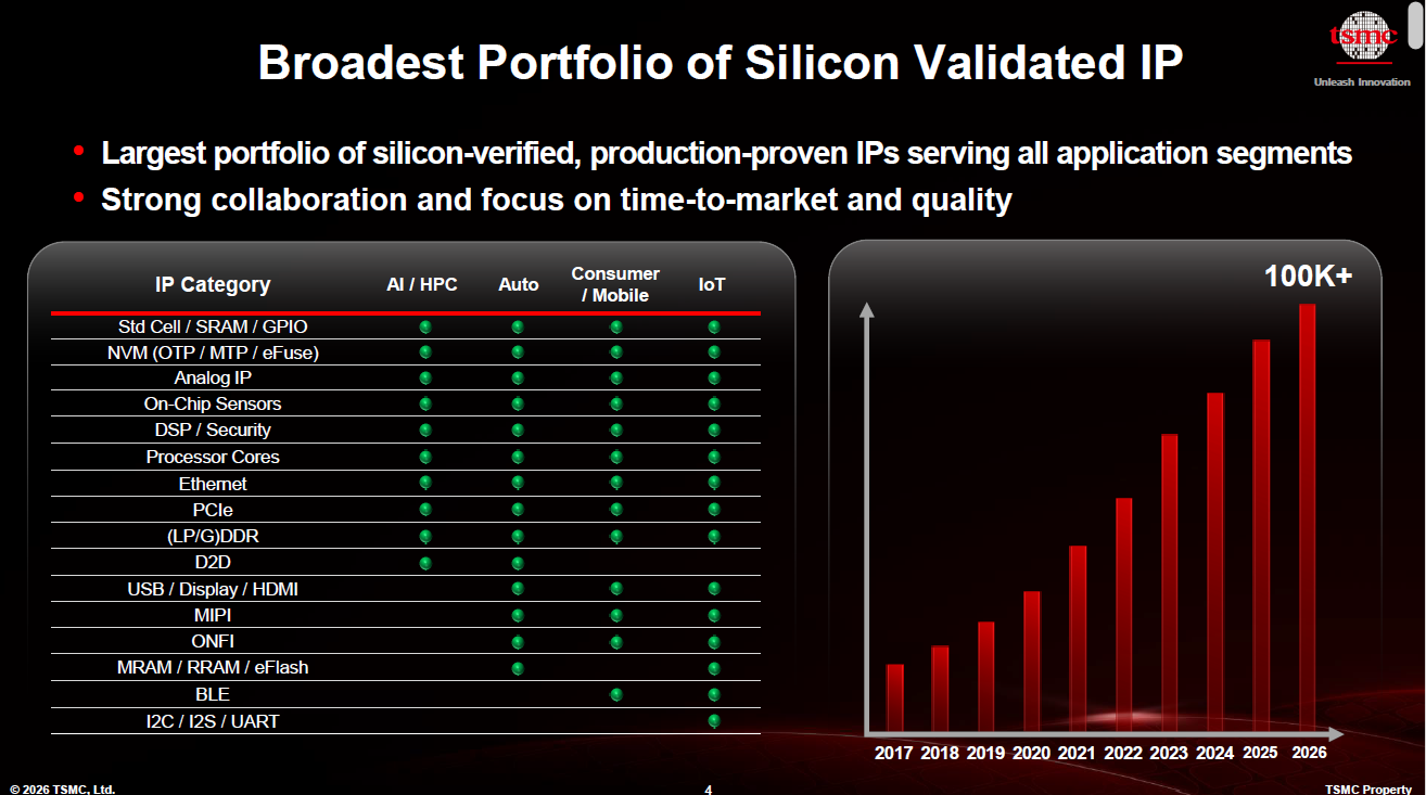
The scale of this ecosystem is best reflected in its portfolio of over 100,000 silicon-verified, production-proven IP titles. This repository isn’t just for the hyperscalers but increasingly targeted at “Physical AI” too for the migration of advanced intelligence into IoT, automotive, and edge devices. By providing these production-proven building blocks, TSMC ensures that the path to a trillion-transistor system is gated by creativity, not by the fundamental physics of IP validation.
Advanced Silicon and the 3D Packaging Backbone
In the AI era, the “one size fits all” approach to manufacturing has been discarded in favor of aggressive Design-Technology Co-Optimization (DTCO). By concurrently refining process, library, and design flow, TSMC’s roadmap delivers a 2.3X power efficiency gain from the current N3P node toward future architectures like A14.
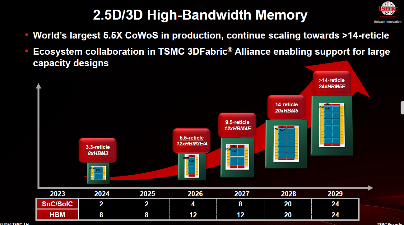
The real breakthrough, however, lies in circumventing the reticle limit. TSMC’s CoWoS® platform is scaling from 3.3-reticle designs to massive packages exceeding 14-reticles. For those visiting the OIP pavilion, the physical 9.5-reticle design on display serves as a tangible milestone of this progress. By 2029, these massive platforms will support 24x HBM5E stacks, enabled by the compounding effect of SoIC (System-on-Integrated-Chips) logic stacking.
Staggering gains are ongoing, from a trajectory moving from a standard SoC on N7 in 2024 to a complex SoIC A14+A14 stack by 2029.
A 48X increase in transistor count within a single CoWoS package over this 5-year window.
An 87X surge in total compute capacity, defined specifically as Transistors × Speed @ Power (normalized performance within a power envelope).
Next-Generation Memory and Connectivity: HBM5 and Silicon Photonics
As AI workloads move from massive training clusters to “Physical AI” and agentic inference at the edge, memory architecture must become more efficient. TSMC is recognizing key partners (SK Hynix, Micron, and Samsung) for their collaboration on the HBM5 standard. By utilizing the TSMC N3P process for the HBM5 base die, the industry is achieving a critical doubling of bandwidth per energy unit.
On the connectivity front, the TSMC-COUPE™ (Compact Universal Photonic Engine) platform is addressing the looming “interconnect wall.” By integrating co-packaged optics and micro-ring modulators (MRM), TSMC is scaling bandwidth density from current 200Gbps production modulators toward a target of 4Tbps/mm by 2030.
Designing “AI for AI”: The Agentic Shift
The most profound shift discussed at the forum was the “virtuous cycle”: using AI to design better chips, which in turn drive more sophisticated AI models.
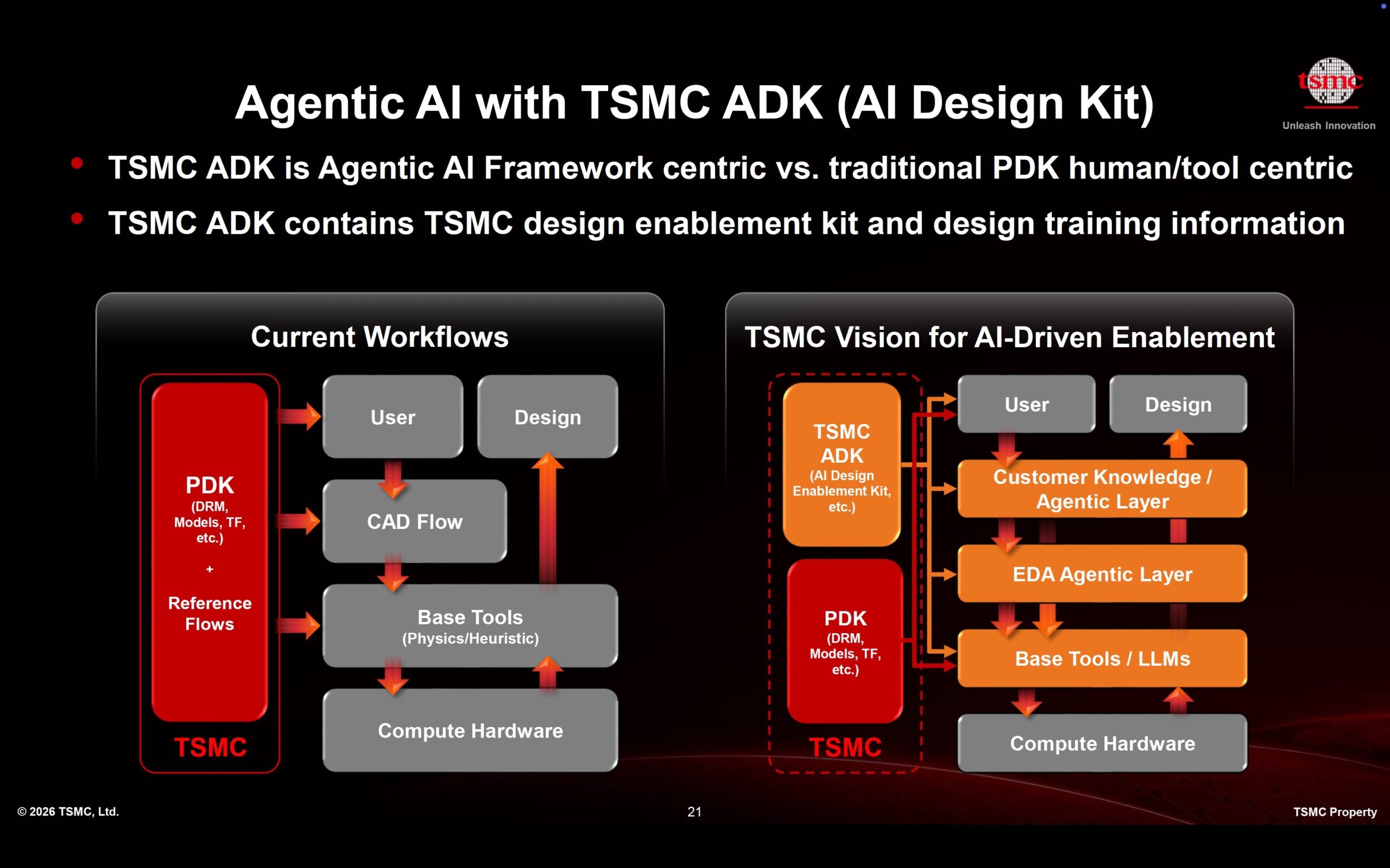
TSMC is evangelizing a transition from the traditional human-centric PDK (Process Design Kit) to the TSMC ADK (AI Design Kit). This is a multi-agent framework where AI agents self-learn from TSMC’s technology learning layers (cell selection, pin escapes and routing strategies) to orchestrate workflows autonomously.
Industry leaders are already seeing the impact through specific agentic tools:
- Digital designers are seeing a 3-5X productivity boost in Place and Route (P&R) iterations
- Analog design migrations (e.g., N5 VCO to N3 VCO) are seeing 3X to 6X productivity gains
Furthering this “AI-native” push, the OIP “Emerging Technologies Alley” featured six hand-picked startups vetted specifically for their innovations in AI-based EDA and IP, signaling a move to bring “AI-first” smaller players into the inner circle of the ecosystem.
System-Level Co-Optimization: From Silicon to SuperPOD
To support trillion-transistor architectures, TSMC is looking beyond the die to the entire rack through STCO (System-Technology Co-Optimization). This holistic approach treats the AI SuperPOD as a single unit of design.
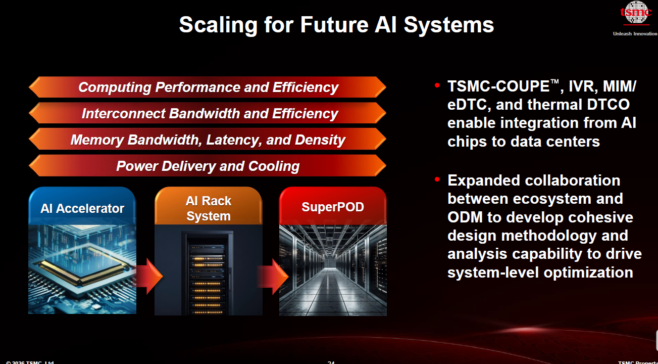
Optimizing a rack-scale system requires more than just logic scaling; it necessitates advanced power delivery and thermal management. TSMC is integrating Integrated Voltage Regulators (IVR), Metal-Insulator-Metal (MIM) capacitors, and Deep Trench Capacitors (eDTC) to stabilize power delivery, while applying thermal DTCO to manage the extreme heat density of next-generation AI accelerators.
Summary
The trillion-transistor era rests on three strategic pillars:
Relentless Logic and Packaging Innovation: Pushing the limits of CoWoS scaling and A14 transistor density.
Radical Design Cycle Acceleration: Implementing the “Agentic AI” shift via the TSMC ADK to compress years of design work into months.
Holistic System-Wide Optimization: Utilizing STCO to align silicon, power delivery, and thermal management into a cohesive system.
As the OIP ecosystem enters its third decade, it remains the vital infrastructure for this Intelligence Revolution. The combination of agentic design flows and massive 3D integration marks the most significant architectural inflection point in a generation.
Also Read:
TSMC’s CoWoS Capacity to Double by 2028—and Rivals Will Still Win Orders
TSMC’s 2026 OIP Forum to Spotlight the Technologies Shaping the Next Era of Chips
ASML and TSMC’s 12-Inch Photomask Initiative: Technical Significance
Share this post via:



Comments
There are no comments yet.
You must register or log in to view/post comments.