





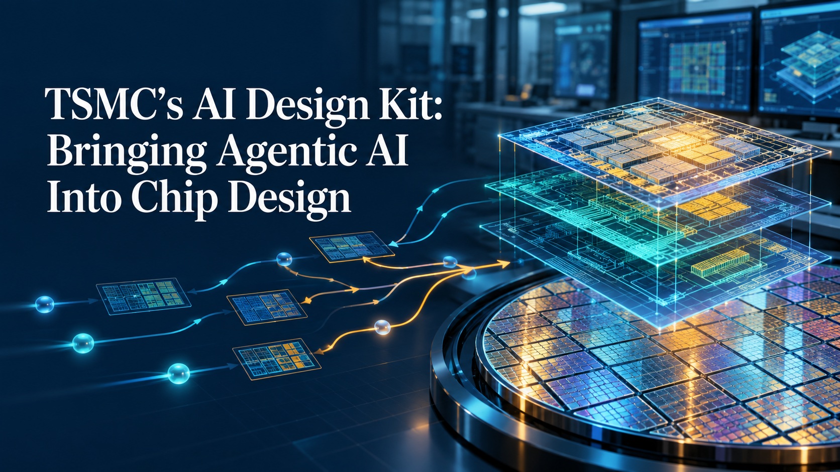
TSMC is introducing an AI Design Kit, or ADK, to help artificial intelligence tools make better use of its semiconductor manufacturing knowledge. The idea is to give AI agents that run chip-design workflows a technology-specific foundation, so they can adjust designs toward performance, power and area targets with less manual iteration. Announced in the context of TSMC’s Open Innovation Platform ecosystem event last week, the ADK points to a shift from AI assisting with isolated design steps toward agents coordinating more of the process.
A conventional process design kit, or PDK, contains the models, rules and files needed to design a chip for a particular fabrication process. TSMC’s ADK serves a different role. According to Aveek Sarkar, a TSMC director responsible for ecosystem and alliance management, it provides a “technology knowledge layer” for agentic design frameworks. In practical terms, an AI-driven tool could draw on that layer as it selects settings, evaluates tradeoffs and repeats electronic-design-automation tasks. TSMC has not publicly described the full contents, interfaces or licensing terms of the kit.
Why is such a layer useful? Chipmakers can start with validated reference flows, but those flows cannot prescribe the best settings for every circuit and product. A team designing an AI accelerator, for example, may prioritize speed and dense integration, while another customer values low power or cost. Engineers typically adjust tools and examine the consequences for timing, energy use and physical layout. At advanced process nodes, these choices interact in complicated ways. A faster feedback loop can make it easier to explore options before a design is finalized for fabrication, a milestone known as tape-out.
TSMC says its ADK will enable agentic AI tools and workflows built on knowledge specific to its technologies. An agent might run a design tool, inspect the result, change parameters and run it again, using measured outcomes to decide what to try next. This is an illustration of the intended workflow, not a published specification of ADK functions. TSMC expects the approach to speed circuit- and architecture-specific optimization and plans to develop it with partners that supply electronic design automation software.
The company has cited productivity gains of three to five times for digital design and up to six times for analog and radio-frequency design in discussing the initiative. Those are TSMC’s stated figures; its public explanation does not give enough detail to treat them as a universal performance benchmark. Results would depend on the design task, the software involved, the starting point and how productivity is measured. The ADK’s value will become clearer as customers and partners describe actual deployments and comparable outcomes.
The project fits within TSMC’s broader Open Innovation Platform, which connects its manufacturing technologies with design tools, intellectual property, cloud services and specialist partners. TSMC has already worked with partners on AI-based design tools and has used reinforcement learning for circuit optimization and design-space exploration. The ADK is intended to help agentic systems use that ecosystem more effectively. At its 2026 ecosystem forum, TSMC highlighted AI-driven automation tools and agentic workflows as ways to handle growing design complexity.
There are limits to what an agent can settle on its own. A design that appears better on one metric may create problems elsewhere, including timing, heat or manufacturability. For multi-die systems, the interactions between chips, packaging and interconnects add further constraints. Engineers still need reliable models, verification and sign-off before a design can be manufactured. TSMC describes the ADK as a way to guide optimization within design workflows, not as a substitute for those checks.
Bottom line: The ADK is best understood as an emerging layer between TSMC’s process expertise and AI-driven design software. If it works as intended, it could shorten the cycle between a design decision and trustworthy feedback. The unanswered questions are concrete: which tools will use it, how much of the workflow agents can control, what information the kit supplies, and whether the claimed gains hold across customer designs.
Also Read:
TSMC OIP Ecosystem Forum 2026: Broadcom’s View of ASICs and Ecosystems
Why Advanced Chip Packaging Is Becoming a Design Problem
Siemens and TSMC push AI deeper into chip design
Share this post via:



Comments
There are no comments yet.
You must register or log in to view/post comments.