





As chipmakers put more computing power into a single system, the challenge extends beyond making individual chips faster. They must connect multiple chips, memory stacks, power supplies, and sometimes optical components in a compact package. In the2026 TSMC OIP Forum talk “Addressing Inter-Die Complexity for 3D Multi-Die Design by Synopsys / Arm”, TSMC describes how that growing complexity is changing the tools used to design chips. Physical layout, electrical performance, heat, and mechanical structure now have to be considered together.
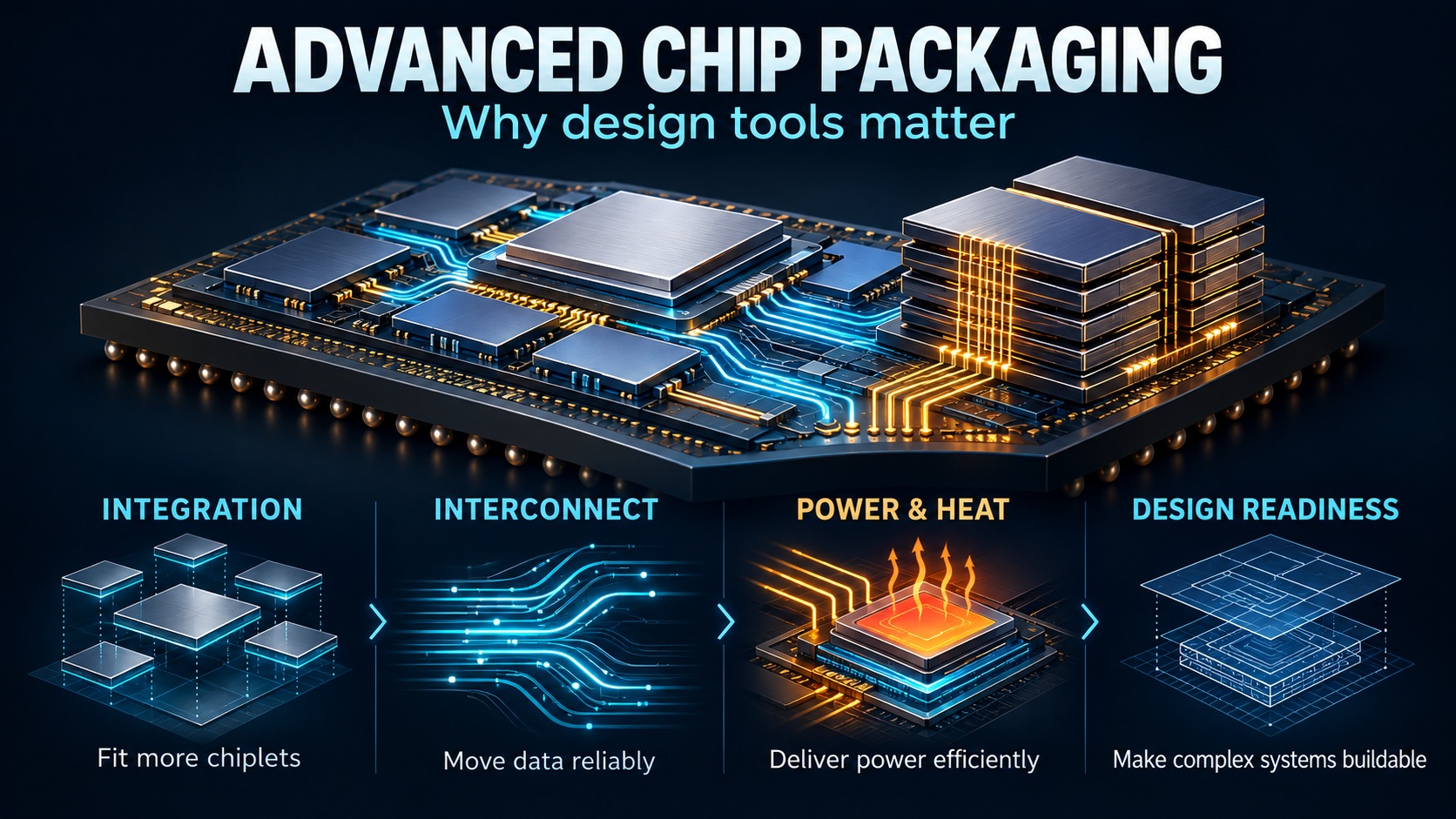
The first challenge is integration. Modern packages can place chiplets side by side and stack them vertically. Connections that pass through silicon, wiring tracks, and the spaces available for standard cells all follow different grids. If those grids are poorly aligned, a connection may block more usable space than necessary. TSMC describes adjusting connection placement to recover space for circuit cells. A small percentage gain can matter when repeated across a large design: it creates room for useful circuitry without requiring a new manufacturing process.
Chiplet placement presents a related problem. Moving one component can force several others to move because of spacing, enclosure, and symmetry rules. The speaker describes work with electronic design automation partners to express those rules in forms that placement software can act on. The talk also describes an AI system that examines remaining rule violations and proposes fixes. In one example, it resolves a spacing violation by changing which edges line up, rather than simply pushing two chiplets farther apart. The practical benefit is less manual rework as packages become more crowded.
The second challenge is high speed communication. Closely packed connections can interfere with one another, weakening signals even when every wire satisfies manufacturing rules. TSMC’s approach is to translate signal quality requirements into routing instructions that software can follow, including shielding and consistent connection shapes. The speaker reports that automated tools routed large groups of signals in minutes where manual work would take much longer. These are results reported in the talk, not a guarantee that every design will see the same improvement. They show why routing software must consider electrical behavior while it lays out wires.
Checking those connections is difficult too. A designer may need to estimate how often a transmitted bit will be read incorrectly, including errors so rare that direct simulation takes too long. The talk describes a statistical method intended to make those checks practical. Faster checks let engineers test more design choices before committing to a layout.
The third challenge is power and heat. More computation in a smaller area demands more power. Sending that power as high current wastes energy and generates heat in the package’s electrical paths. TSMC describes placing voltage conversion closer to the computing chips so power can travel farther at a higher voltage and lower current. That can reduce losses, but it adds components that must be modeled. The speaker says simplified, layered models have reduced simulations that once took more than a month to a matter of days.
Heat also becomes harder to predict as chip structures and materials change. A model that spreads heat evenly across a circuit cell can miss hot spots near its active parts. The talk describes more detailed thermal models for new power structures, metal wiring, and optical components. Accurate temperature estimates are especially important when optical behavior changes with heat.
Finally, the speaker emphasizes design readiness. A promising packaging technology is only useful if engineers have reliable rules, models, and software to design with it. TSMC says it has tested these materials with tool partners and found issues involving capacity, runtime, and accuracy. That work may sound less dramatic than a new chip architecture, but it determines whether customers can build complex products predictably.
Bottom line: Progress in computing increasingly depends on making many components work as one system. Better placement preserves scarce space; better routing supports faster communication; better power delivery limits wasted energy; and better models reveal problems before fabrication. The talk’s central message is that advanced packaging needs an equally advanced design process. As systems grow denser, gains will come from coordinating manufacturing technology and design tools across the whole package.
Also Read:
Share this post via:




Comments
There are no comments yet.
You must register or log in to view/post comments.