







Recently, I had the opportunity to speak with Johann Foucher, founder and CEO of Pollen Metrology, a French company whose journey offers a rare vantage point on how artificial intelligence is reshaping semiconductor manufacturing from the inside out. What makes Pollen Metrology’s story compelling isn’t just the technology itself, but the timing and conviction behind it: the company placed its bet on AI-driven metrology and process control roughly a decade before the current wave of industry-wide AI adoption made such an approach seem inevitable.
Today, that early bet has matured into something distinctive: a Collaborative AI Platform built specifically for the fragmented world of semiconductor and advanced materials manufacturing, an industry where data lives in silos, tools rarely speak the same language, and no single company controls the full picture. Foucher’s approach addresses that fragmentation directly, offering a way for manufacturers, equipment makers, and materials suppliers to pool intelligence without pooling proprietary secrets.
The following is a summary of our cordial discussion, covering the origins of Pollen Metrology, the technical philosophy behind its platform, and where Foucher sees AI-driven metrology heading next.
A Ten-Year Plan, Delivered on Schedule
When Pollen Metrology was incorporated in France in 2014, its founder and CEO, Johann, set an unusually patient roadmap for a deep-tech startup: ten years to bring a fully matured technology platform to market. That timeline wasn’t a rough estimate, it was the explicit plan presented to investors during the company’s 2017 fundraising round. Fast forward to 2024, and Pollen hit that mark almost exactly as promised. The company’s “Smart” software platform, now in its third generation, is fully matured and operating in production environments across the semiconductor and advanced materials industries.
Getting there wasn’t a straight line. Pollen spent years developing three successive generations of its Smart platform, working with limited funding and a small customer base while the technology matured. That patience is now paying off. According to Johann, last year marked a pivotal moment for the company: the point where years of R&D investment got validated by real market traction.
The Positioning: A Collaborative AI Platform for a Fragmented Industry
Pollen describes Smart 3 as a collaborative AI platform built specifically for the semiconductor industry and advanced materials manufacturing.
The core problem it addresses is one that will be familiar to anyone who has worked inside a fab or an equipment supplier: the semiconductor lifecycle, from input selection and design of experiments, through process execution, to process control, metrology, inspection, and yield optimization, is fractured across silos. Different teams, different software tools, different databases, different KPIs. At every handoff between these silos, critical engineering knowledge gets lost.
Smart 3 is designed to be the connective layer across that entire lifecycle, linking engineers, equipment, and manufacturing operations into a single continuous loop rather than a series of disconnected steps.
One Platform, Any Data, Any Equipment
A defining technical characteristic of Smart 3 is its ability to ingest virtually any data type relevant to materials science and semiconductor manufacturing: optical data, spatial data (wafer- or pattern-level), 3D surfaces and profiles, high-resolution imaging (SEM, TEM, optical), process-equipment signals, and process context such as recipes and material properties. Rather than requiring a different tool for each data source, Smart 3 is built as a single platform capable of handling all of them, letting customers start with one data source and progressively expand the platform into new process areas as needs evolve.
Just as important as the data coverage is the platform’s openness. Pollen provides a software development kit (SDK) that allows customers to extend Smart 3 in two directions: process engineers, application experts, and manufacturing teams can build on top of it directly, while data scientists, AI developers, or technology partners can integrate their own proprietary algorithms and IP. The platform is deployed on-premises rather than in the cloud, and all customer IP remains fully protected, meaning each customer effectively ends up with its own tailored version of the software.
Closing the Loop Between R&D and Fabrication
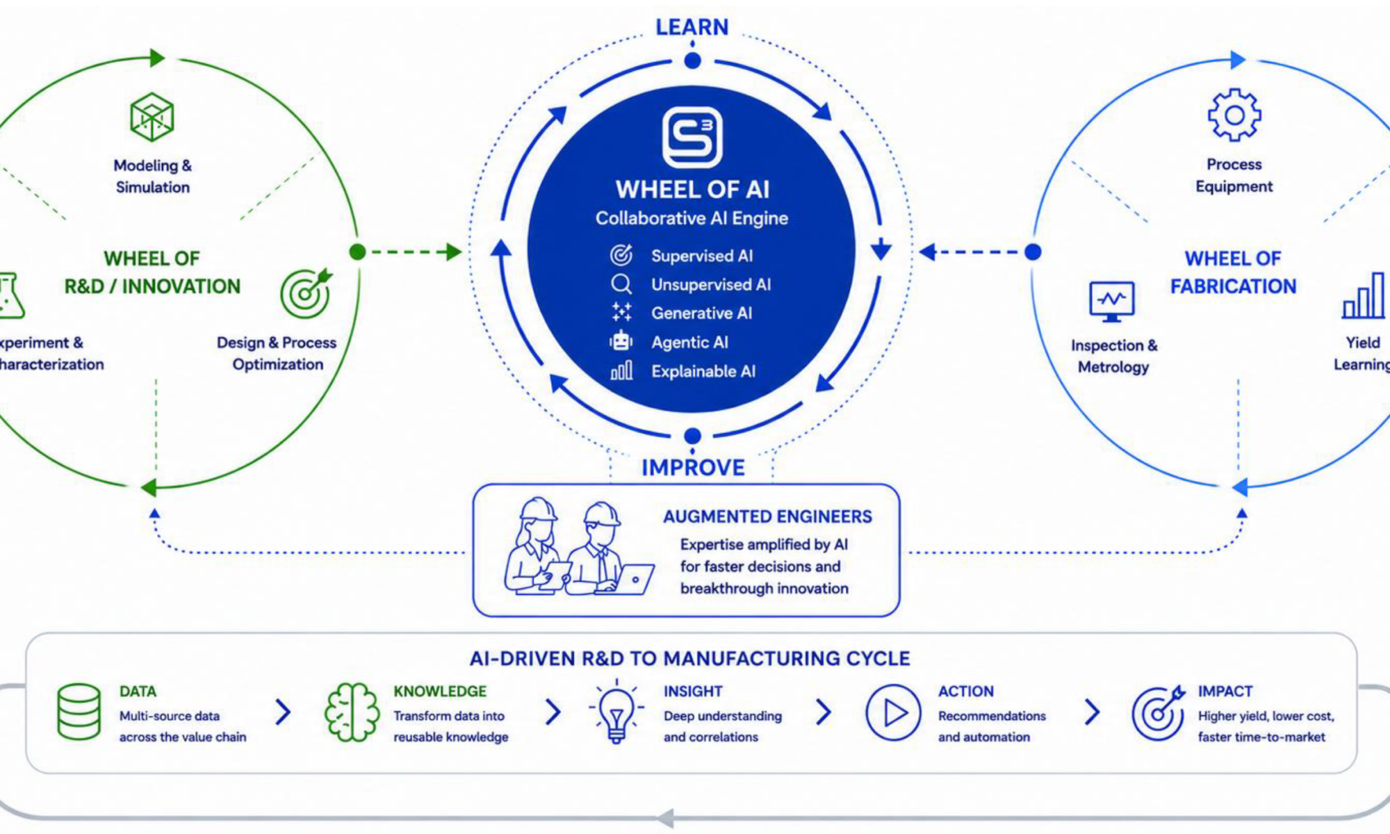
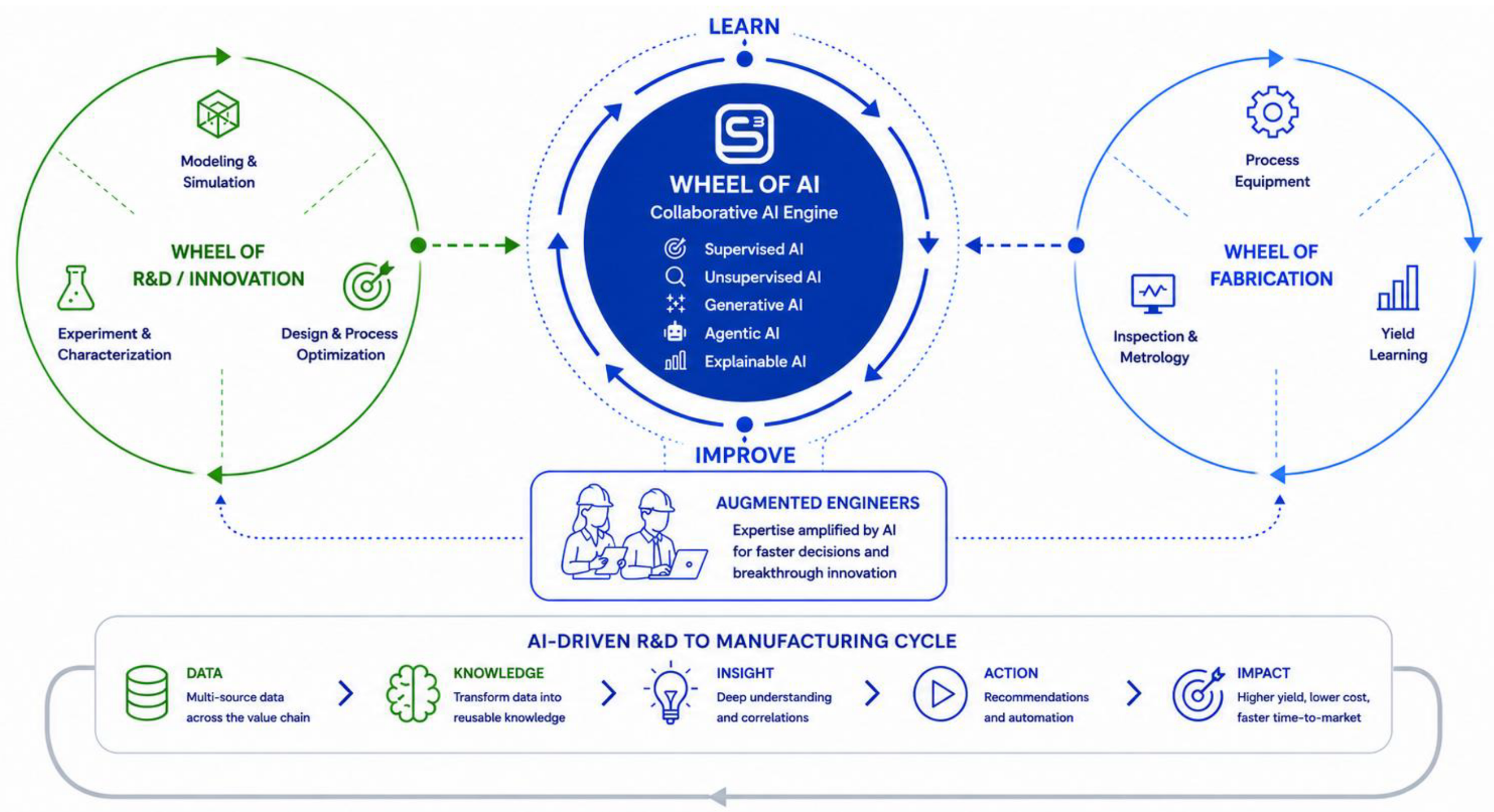
Johann frames Pollen’s broader ambition in terms of two traditionally disconnected “wheels”: the wheel of R&D and innovation, and the wheel of fabrication. Today, these operate largely in isolation. Smart 3’s goal is to build an automated link between them, what Pollen calls the “wheel of AI”, combining multiple AI approaches with engineering knowledge to create a continuous, self-improving loop connecting research and manufacturing. See figure 1.
This also reflects how Pollen positions itself relative to customers’ internal AI strategies. Most of Pollen’s customers already have data scientists building their own supervised, unsupervised, generative, or agentic AI tools. Pollen’s value isn’t in replacing those efforts, rather, it’s in orchestrating them. Customers can choose a fully turnkey solution from Pollen, or take the underlying software architecture and SDK and integrate their own AI tools into it, with Pollen managing the platform architecture either way.
Where Pollen Fits in the Manufacturing Flow
To understand why Pollen’s platform matters, it helps to unpack what actually happens on the back end of semiconductor manufacturing, the stages after a wafer has been processed through hundreds of lithography, etch, and deposition steps, where the job shifts from *building* the device to *proving* it was built correctly and *fixing* what wasn’t. This is the domain Smart 3 lives in, and it breaks down into four connected disciplines.
Metrology: Measuring What Was Actually Built
Metrology is the measurement of physical structures on the wafer, critical dimensions (CD), film thickness, overlay accuracy between patterned layers, and 3D profile shape. It’s the difference between a design that says a transistor gate should be 14 nanometers wide and confirming that it actually came out that way across millions of dies.
Three techniques dominate:
- CD-SEM (Critical Dimension Scanning Electron Microscopy) fires a focused electron beam at the wafer surface and images the resulting secondary electrons, producing a top-down picture precise enough to measure feature widths at the nanometer scale. It’s fast and non-destructive, which makes it the workhorse for high-volume in-line measurement.
- TEM (Transmission Electron Microscopy) goes further: a thin cross-section is sliced out of the wafer and electrons are transmitted through the sample, revealing internal structure, layer stacks, interfaces, voids, that a top-down SEM image can’t show. It’s destructive and slower, so it’s used selectively, often to calibrate or validate what CD-SEM is seeing at scale.
- Optical metrology (scatterometry, ellipsometry) uses reflected or scattered light to infer dimensions and film properties indirectly, through modeling. It’s the fastest of the three and well suited to blanket, high-throughput monitoring, at the cost of requiring good models to interpret the signal correctly.
This is precisely the data Smart 3 is built to unify, Pollen’s platform is designed to ingest CD-SEM, TEM, and optical data side by side rather than treating each as a separate silo requiring its own analysis tool.
Inspection: Finding What Went Wrong
Where metrology measures dimensions, inspection hunts for defects, particles, scratches, pattern collapses, voids, or bridging shorts that shouldn’t be there at all. Inspection tools scan wafers (or sampled dies) at high speed, flag anomalies, and classify them by type and severity, since a random particle defect and a systematic lithography defect point to very different root causes.
The hard part isn’t detection so much as classification and triage: a modern fab can flag thousands of potential defects a day, and distinguishing the handful that indicate a real process excursion from routine background noise is what separates useful inspection from an alert fatigue problem. This is where AI-based image classification, the kind Pollen’s toolbox applies, as in its published work with STMicroelectronics on automated TEM image processing, replaces slow, inconsistent manual review with models trained to recognize defect signatures automatically.
Root-Cause Analysis: Connecting Symptoms to Causes
Once a defect or an out-of-spec measurement is flagged, the next question is why. Root-cause analysis correlates metrology and inspection results against upstream process data, equipment logs, recipe parameters, chamber conditions, even which tool or chamber a wafer passed through, to trace a symptom back to its source.
Historically this correlation work has depended on engineers manually cross-referencing spreadsheets and tool logs across disconnected databases, which is exactly the kind of siloed handoff Pollen’s platform is built to eliminate by keeping process context attached to the measurement data from the start.
Yield Optimization: Closing the Loop
Yield, the percentage of dies on a wafer that function correctly, is the commercial bottom line all of the above feeds into. Yield optimization uses aggregated metrology, inspection, and root-cause data to identify systematic issues suppressing yield and to feed corrective adjustments back into the process recipe, closing the loop between what the fab measures and what it does next.
This is also where digital twins, virtual models of a process or a piece of equipment, come in: instead of only reacting to defects after the fact, engineers can simulate the effect of a process change against the digital twin before committing it on real wafers. Pollen’s collaboration with STMicroelectronics paired its AI image-processing toolbox directly with ST’s digital twin technology, and the result was concrete: a 50% improvement in process window, with critical-dimension variability dropping from 25% to 12%, en route to a target specification of 7%.
Taken together, these four stages, metrology, inspection, root-cause analysis, and yield optimization, are usually run by separate teams on separate tools with separate databases in a typical fab. Smart 3’s core bet is that connecting them into one continuous loop, rather than four disconnected ones, is where the next real gains in fab productivity are sitting.
A Customer Base Spanning Chipmakers, Equipment Suppliers, and Research Institutes
Pollen’s customer base today spans IC makers and fabs, equipment suppliers, and companies in photonics, AR/VR, display, and micro-LED. It has also begun working with research institutes and universities, including CEA-Leti in Grenoble, and a new collaboration involving IMEC.
Several reference customers illustrate the platform in action:
- Meta has co-published work with Pollen on AR/VR applications, including 3D model reconstruction combining top-down CD-SEM and cross-section imaging.
- STMicroelectronics has published jointly with Pollen on automated image processing for TEM, pairing Pollen’s image-processing AI toolbox with its digital twin technology to close the loop on edge-process modernization. The result: a 50% improvement in process window, with critical-dimension variability dropping from 25% to 12%, en route to a target specification of 7%. STMicroelectronics has since expanded its use of the platform to inspection transfer learning, reusing AI models trained on one generation of fab tools to accelerate deployment on newer tool generations with minimal retraining.
- Equipment makers, including Infinitesima (UK) with its high-speed AFM technology, are embedding Pollen’s SDK directly into their equipment to build automated application software, reportedly developing new applications roughly 10 times faster than developing comparable capabilities in-house.
Beyond these partners, Pollen collaborates with additional tool suppliers, fabs, and fabless companies on Digital Twin technology, correlative metrology, and agentic AI. Together, these efforts aim to enhance tool capabilities and fab automation, driving the semiconductor industry toward full lights-out manufacturing.
From Metrology to a Full Yield-Optimization Toolbox
On top of the core SDK, Pollen offers a growing set of pre-built application modules covering metrology, inspection, and process optimization, including digital twins, root-cause analysis, and yield enhancement tools. Customers typically start with one capability, such as metrology, and progressively layer in defect analysis and yield optimization as their use of the platform matures. Deployments can be embedded directly into a fab’s operations or integrated into a specific piece of equipment, depending on the customer’s needs.
A Structured Path to Adoption
Pollen has formalized how new customers engage with the technology, through what it calls the Pollen Academy onboarding journey:
Learn (1–3 days): foundational training and use-case identification.
Discover (2–3 months): customers assess the technology independently, with no bespoke development required.
Explore (6 months): Pollen provides the technology with weekly updates and support, refining it against the customer’s specific application.
Deploy (12 months): once ROI is demonstrated, the platform moves into full production, in a lab, pilot line, single fab, or across multiple fabs.
The intent behind this staged approach is straightforward: to prove, with each customer, that adopting Pollen accelerates technology development, qualification, and yield ramp-up compared with building similar capability internally.
The Build-vs-Buy Case
For companies considering building their own AI-driven process-data platform in-house, Pollen makes a pointed cost-and-speed argument. Building a comparable capability internally requires years of development, a substantial software team, and, even with modern LLM-assisted coding, the overhead of selecting technologies and building out a complete software stack, since a production-grade AI solution is far more than an algorithm.
With Pollen’s SDK, customers such as Infinitesima have instead been able to stand up new applications in a matter of weeks, or in some cases days, using small internal teams, while retaining full ownership of their own IP and the ability to scale the platform across their own customer base.
Looking Ahead
After a decade of patient technology development, Pollen Metrology now presents itself less as an emerging startup and more as an operationally proven platform company, one with a maturing product, an expanding and increasingly high-profile customer list, and a clear thesis on where the semiconductor industry’s AI strategy is heading: not toward more disconnected point tools, but toward orchestration across the entire manufacturing and R&D lifecycle.
Also Read:
ASML Has High-NA and Chipmakers Can’t Say No
High-NA EUV Moves From Experiment to Manufacturing
ASML and TSMC’s 12-Inch Photomask Initiative: Technical Significance
Share this post via:



Rethinking Phase Jitter: An Algorithmic Approach to Signal Integrity