


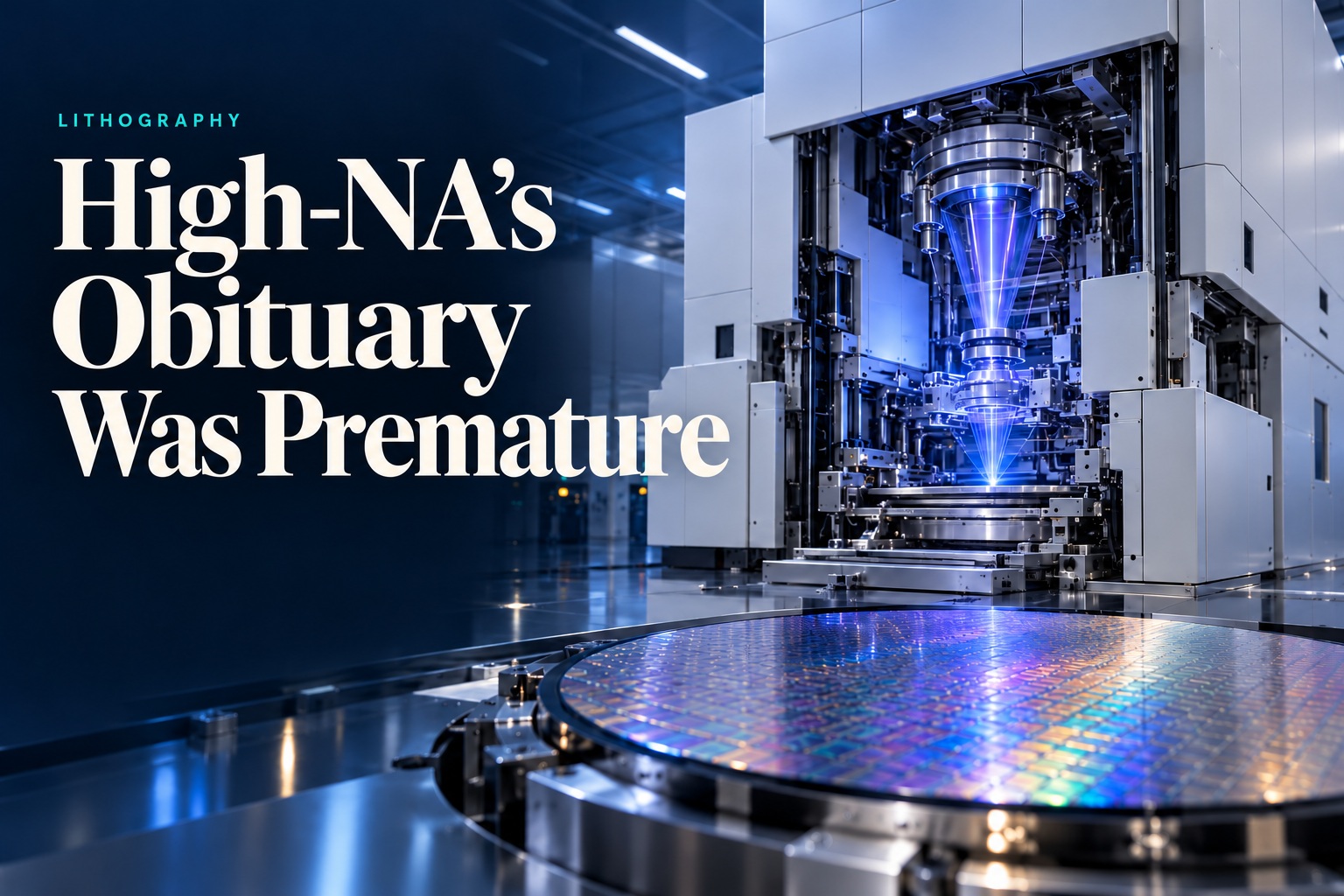




High numerical aperture EUV lithography was supposed to be the next step in semiconductor manufacturing. Then came the doubts: expensive scanners, smaller exposure fields, difficult economics and big customers finding ways to stretch existing equipment. It became tempting to confuse a delayed adoption curve with a technology running out of road.
Recent announcements make that conclusion harder to defend. Intel is shipping products patterned partly with High-NA. Samsung has outlined a production timetable. TSMC has recently announced plans to adopt and joined an effort to address one of the technology’s structural limitations. High-NA still has plenty to prove, but its obituary looks premature.
The strongest evidence comes from Intel. In July, ASML announced that selected layers of a subset of Panther Lake processors were being manufactured using High-NA EUV. Those layers were dual-qualified against conventional EUV, with yields matching the existing NXE platform. That matters more than a demonstration wafer: it places the technology inside a shipping product flow, where repeatability, availability and manufacturing discipline become unavoidable requirements. It does not mean every Panther Lake processor uses High-NA, or that Intel 18A depends on it.
By September, Intel and ASML reported more than one million wafers processed across certification, research, development and production. That qualification matters: the figure is not one million customer production wafers. Nevertheless, the companies said overlay, throughput and availability were meeting Intel’s expectations. The useful signal is accumulated operating experience, rather than a single impressive number. High-NA is moving from proving that it can print toward proving that it can earn its place in a factory.
The underlying attraction remains straightforward. Increasing numerical aperture from 0.33 to 0.55 improves resolution, allowing finer features to be patterned. Where that replaces multiple exposures and associated processing steps, the economics can extend beyond scanner throughput. Fewer operations can potentially reduce process complexity and opportunities for variation. The relevant comparison is therefore the cost and yield of the complete patterning sequence, rather than the purchase price of one machine. Whether those benefits materialise remains specific to the layer and manufacturing process.
The complications are equally real. High-NA’s anamorphic optics halve the exposure field when using today’s mask format. Large designs consequently face layout constraints or stitching requirements. Intel says current masks remain usable through appropriate floorplanning and its stitching solutions. Longer term, ASML and TSMC are pursuing 12-inch photomasks, with a pilot line targeted for 2031 and advanced-node production readiness for 2033. Those dates show both industry commitment and the amount of ecosystem work still ahead.
TSMC’s position is particularly revealing. The company intends to introduce High-NA into advanced-node volume manufacturing starting in 2030. On its October earnings call, chairman and chief executive C.C. Wei emphasised maturity and reasonable cost as conditions for adoption. That is consistent with a manufacturer choosing its insertion point according to production economics. Being first to install a tool and being first to extract an attractive return are different achievements.
Samsung, meanwhile, plans to introduce High-NA into DRAM volume manufacturing by 2028. Together, these schedules suggest staggered adoption across customers and applications, rather than a universal switchover. Existing EUV will continue improving and competing for layers. High-NA must win each allocation through measurable manufacturing advantages.
Bottom line: For chipmakers, the next questions are practical: which layers benefit, how reliably the scanner runs, what changes are required upstream and downstream, and whether savings survive full production accounting. Those answers will determine deployment speed more convincingly than either launch announcements or sceptical headlines. The evidence increasingly supports High-NA’s future, while leaving its commercial pace open. The technology has gained credibility through production experience, but broad adoption will still require sustained, demonstrable economic value at scale.
Also Read:
Smoothing the Quantum Path: ASML and Xanadu Target Photon Loss
Siemens and NVIDIA Accelerate Lithography for Next-Generation AI Chips
Maskless EUV Lithography: An Alternative to E-Beam
Hyper-NA EUV: The Next Frontier in Chipmaking Could Arrive in 2036
Share this post via:


TSMC’s Patent and the Harsh Realities of 3D DRAM Competition