







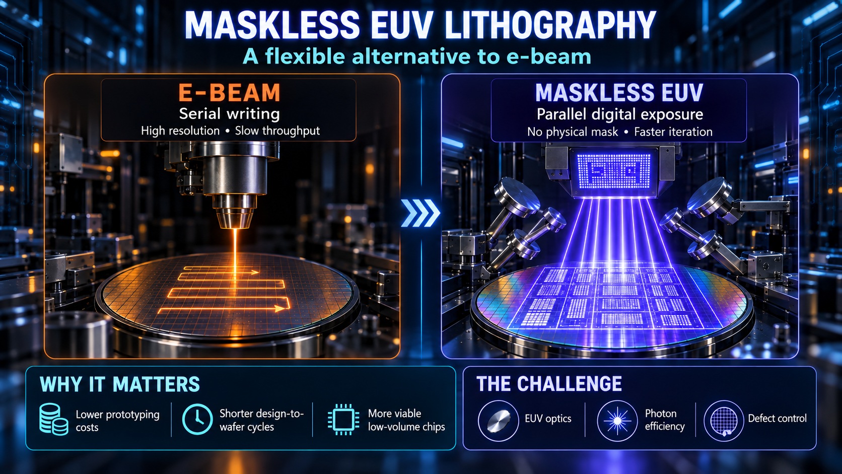
Semiconductor manufacturing depends on lithography: the process of transferring tiny circuit patterns onto a silicon wafer. Conventional extreme-ultraviolet (EUV) lithography projects light with a wavelength of 13.5 nanometers through a reflective optical system, using a custom photomask to define each layer. It can print extraordinarily small features at high throughput, but every new design requires an expensive, carefully manufactured mask set. Maskless EUV lithography proposes a different approach. Instead of storing the pattern on a physical mask, it would use a programmable array or another rapidly addressable optical element to write digital patterns directly onto the wafer.
The idea occupies an important middle ground between conventional EUV and electron-beam lithography. E-beam systems are also maskless and can draw extremely fine features, making them essential for research, prototyping, and producing the masks used by optical lithography. Their weakness is speed. An electron beam generally writes patterns serially, point by point or shape by shape. A modern chip contains an immense number of features, so exposing a full wafer can take far too long for practical manufacturing. Parallel multibeam systems improve throughput, but they introduce substantial complexity in beam control, calibration, data handling, and defect management.
A maskless EUV platform could combine direct digital patterning with the parallel exposure advantages of light. In principle, millions of controllable elements could expose many features simultaneously, avoiding the serial bottleneck of a single e-beam. Designs could be changed by loading a new pattern file instead of fabricating a new mask. That would shorten iteration cycles and lower the fixed cost of producing small quantities. Researchers could test several layouts quickly, startups could prototype advanced chips without purchasing a complete mask set, and manufacturers could economically produce specialized devices in volumes too low for conventional EUV.
This flexibility is why the technology matters. Mask costs and lead times increasingly shape who can experiment at the leading edge. When each design revision carries a large upfront expense, companies are encouraged to make fewer, safer bets. Maskless EUV could support more frequent experimentation, customized accelerators, small-batch photonics, secure or locally produced chips, and late-stage personalization. It could also reduce the economic penalty of correcting a design error. In an industry where learning speed is a competitive advantage, faster design-to-wafer cycles may be as valuable as smaller transistors.
The approach, however, is not a simple replacement for either EUV scanners or e-beam tools. EUV radiation is strongly absorbed by most materials, so the system must operate in vacuum and rely on specialized reflective optics. A programmable pattern generator must survive EUV exposure while switching with exceptional precision. It must deliver adequate optical power, maintain nanometer-scale placement accuracy, control heat and contamination, and avoid adding defects. Photoresist behavior creates another challenge: at very small dimensions, limited photon counts produce stochastic variation, including rough edges, missing contacts, or unintended bridges. Vast pattern files must also be processed and delivered in real time.
For these reasons, the first successful applications would likely be selective rather than a wholesale takeover of high-volume lithography. Maskless EUV may initially serve rapid prototyping, low-volume advanced devices, research, mask repair, or particular critical layers where flexibility justifies lower throughput. E-beam would remain valuable for the finest direct-write work and mask production, while masked EUV would retain its advantage for manufacturing millions of identical chips.
Bottom line: Even within that narrower role, maskless EUV could change semiconductor innovation. It attacks a growing mismatch: fabrication tools can create remarkable structures, yet the cost and delay of preparing masks restrict access to them. By turning patterns from physical infrastructure into software-controlled inputs, the technology could make advanced lithography more adaptable and accessible. Its importance is therefore not merely technical. Maskless EUV could alter the economics of experimentation, broaden participation in chip design, and help the semiconductor industry move from rigid mass production toward faster, more varied, and more responsive manufacturing for many emerging applications worldwide.
Also Read:
High-NA EUV Moves From Experiment to Manufacturing
ASML and TSMC’s 12-Inch Photomask Initiative: Technical Significance
Five Billion Pulses Later: What DUV Optics Testing Reveals About Semiconductor Tool Uptime
Share this post via:




TSMC’s AI Expansion Signals a Broader Shift in Computing