




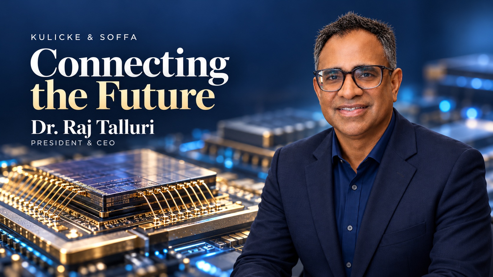



Dr. Talluri joined K&S in August 2026 as a member of the Board and assumed the role of President and Chief Executive Officer of K&S in September 2026. Prior to joining K&S, Dr. Talluri served as President, Chief Executive Officer and a member of the Board of Directors at Enovix Corporation, a Nasdaq-listed advanced battery technology company. Prior to Enovix, Dr. Talluri served as Senior Vice President, General Manager, Mobile Business Unit at Micron Technology. Dr. Talluri has a strong background in semi, having served in various senior executive roles at Qualcomm CDMA Technologies and a variety of engineering and business leadership roles at Texas Instruments Incorporated.
Tell us about your company
I am honored to lead Kulicke & Soffa at a truly special moment. We are celebrating our 75th anniversary this year. We were founded in 1951, and for three-quarters of a century we have been at the heart of how the world’s semiconductors get connected and packaged. Today we are headquartered in Singapore and Fort Washington, Pennsylvania, and our equipment touches virtually every chip made, from ball and wedge bonders to advanced Fluxless Thermo-Compression Bonding, vertical wire, dispensing, and wafer-level bonding systems.
I joined as CEO in September, and I stepped into a business that is currently firing on all cylinders. Our most recent quarter, fiscal Q3 2026, was one of our strongest quarters in years , where we reported a net revenue of $330.4 million, up 123% year-over-year, with gross margin of 47.8% and non-GAAP EPS of $1.20, beating expectations. We are guiding to roughly $375 million for the fourth quarter of fiscal 2026 ending October 3, 2026 as demand strengthens across general semiconductor, memory, automotive, and industrial markets.
What excites me most is that this momentum comes at a time when K&S is exceptionally well positioned to extend its market leadership in wire bonding, leverage its deep customer relationships and technology expertise, and drive the next phase of growth across advanced packaging and semiconductor assembly solutions.
What problems are you solving
Moore’s Law at the transistor level is getting harder and more expensive every year. As a result, the industry has shifted its focus towards advanced packaging techniques, which entails the stacking of chiplets, HBM memory, and logic in a sophisticated manner instead of merely shrinking transistors. Advanced packaging presents a fundamentally different engineering problem from traditional packaging. How do you bond dies with sub-micron precision, manage warpage and thermal stress, and still hit the throughput and yield numbers needed to build AI processors and HBM stacks at volume?
At the same time, we can’t forget where our roots are. Most chips shipped today, in data centers, cars, consumer appliances, PCs, and smartphones, still rely on traditional wire bonding, to which K&S is both pioneer and a market leader. My job is to make sure we excel across the two prongs: continue to be the recognized leader, and a reliable, high-volume workhorse for traditional packaging, and strive towards becoming a serious innovator in advanced packaging for the AI era.
What application areas are your strongest
I will break it down to 3 areas.
- Traditional packaging (in other words, ball and wedge bonding) is where we’re unquestionably the market leader. Over 75 years, we have built an extensive install base globally, serving foundry service providers, other electronics manufacturers, and automotive electronics suppliers, in addition to OSATs (Outsourced Semiconductor Assembly and Test providers) and IDMs (Integrated Device Manufacturers). This remains our foundation.
- K&S is a leading supplier of advanced wire bonding solutions used in the production of NAND flash, LPDDR memory, and DRAM devices, supporting many of the world’s largest memory manufacturers. Our expertise extends from high-volume wire bonding for NAND and LPDDR packages to advanced multi-stack DRAM applications, where precision, productivity, and reliability are critical. As memory architectures become more complex, driven by AI, high-performance computing, and data center demand, K&S continues to innovate with solutions that enable higher interconnect density, improved package performance, and lower manufacturing costs. Leveraging on our foundation, we continue to drive innovation. For example, we’ve just expanded our ProMEM suite, which delivers up to 20% higher throughput for stacked memory, and we continue to advance our Vertical Wire technology on the ATP MEM PLUS platform to increase interconnect density and is well positioned to support the LPDDR market as it migrates to a stacked die package.
- Advanced packaging for AI/HPC is where I am personally spending a lot of time. Our APTURA TCB platform and our Fluxless Thermo-Compression (FTC) technology, the industry’s first commercially available and high-volume production proven fluxless TCB, are gaining strong traction for chiplets, HBM, and now Co-Packaged Optics as networking moves toward silicon photonics.
What keeps your customers up at night?
There’s a long list, but if I had to summarize it in one sentence, it’s this:
How do we continue delivering more performance at lower cost while managing increasing manufacturing complexity?
Customers are under enormous pressure to shorten development cycles, improve yields, increase throughput, and qualify new technologies faster than before.
For leading-edge production, packaging and assembly have become critical drivers of product performance. A small process variation can affect yield, reliability, power consumption, and cost. For many customers, the ability to ramp production quickly in tandem with manufacturing quality is becoming competitive differentiators.
Another major concern is scalability. Many have demonstrated advanced packaging concepts in a lab-like controlled environment but scaling them to high-volume manufacturing across a fleet of tools, is another question. This is why process expertise, equipment capability, and production know-how, to which K&S has amassed through its APTURA TCB platform and Fluxless Thermo-Compression (FTC) technology, becomes increasingly valuable.
Our job is to help customers move faster and with greater confidence.
What does the competitive landscape look like and how do you differentiate?
The semiconductor equipment industry is highly competitive, and our customers have alternative options in many of the markets we serve. We welcome this competition because it continuously pushes us to innovate and truly understand the overlaps of a broad range of customer challenges.
Many companies can build equipment. What customers increasingly value is a partner that understands the process technology and can help optimize yield, throughput, cost, and reliability.
In this light, K&S’ competitive edge continues to be a strong combination of specialized process expertise, an extensive install base, detailed application knowledge, and close customer collaborations.
We also have a unique advantage because we participate across multiple interconnect and assembly technologies. That gives us visibility to where the industry is headed, allowing us to better assist customers to navigate the significant technology transition into heterogeneous integration.
In advanced packaging specifically, our leadership in Fluxless Thermo-Compression technology, heterogeneous integration applications, and next-generation assembly solutions position us extremely well as AI, memory, and high-performance computing are critical to driving industry level assembly capability.
Our ambition at K&S is to reinvent possibilities by shaping the future of semiconductor assembly and packaging leveraging market-leading technologies with process expertise to deliver measurable value for customers.
What new features or technologies are you working on?
Across our innovation portfolio, our focus is on enabling customers to deliver increasingly complex devices through higher-density packaging, enhanced performance, and improved manufacturing productivity.
We’re continuing to advance our thermo-compression bonding portfolio, including technologies that support increasingly sophisticated heterogeneous integration and future interconnect architectures.
We’re also investing in memory-focused solutions, vertical wire technologies, advanced power semiconductor assembly, and next-generation dispense platforms.
Another area that excites me is the increasing role of software, analytics, AI, and process intelligence. Customers want actionable insight, predictive process control, and faster optimization. Those capabilities can significantly improve factory productivity and overall equipment effectiveness.
How do customers normally engage with your company?
With a 75-year history in the industry, we have built enduring relationships with many of the world’s leading semiconductor manufacturers. Our engagement often begins well before a production tool is installed, as customers look to K&S as a trusted partner in solving complex technology and manufacturing challenges.
In many cases, we engage with customers years before a technology reaches volume manufacturing, working side-by-side to define future requirements, overcome technical challenges, and accelerate commercialization.
That collaborative model has been a hallmark of K&S for decades and has been a recipe for success. Customers value us for being more than an equipment manufacturer, we work closely with customers to help them develop scalable manufacturing solutions.
Once a technology moves into production, we support customers through process optimization, applications engineering, service, software, analytics, and lifecycle support. Because many of our technologies have become deeply integrated into customer manufacturing flows, these relationships often extend for many years, and we are grateful for the trust and long-term support from our customers and business partners.
Ultimately, our success will be measured not only by the tools we deliver, but by the value we create for our customers. We aim to be a strategic partner that helps shape the future of semiconductor innovation, enabling our customers to move faster, innovate with confidence, and succeed in an increasingly competitive market.
CONTACT K&S
Also Read:
From Cloud to Silicon: IC-Link and TSMC Open the Door
Intel Foundry: AI performance now depends on the whole system
Managing Power, Performance and Reliability in the Chiplet Era
Share this post via:



TSMC’s AI Expansion Signals a Broader Shift in Computing